
Microcontrollers Data Sheet


MC68HC(7)08KH12 — Rev. 1.1 Advance Information
Freescale Semiconductor
29
1.5.2 Power Supply Pins (V
DDA
, V
SSA
, V
DD1
, V
SS1
, V
DD2
, and V
SS2
)
V
DDA
and V
SSA
are the analog power supply and ground pins used by
the on-chip Phase-Locked Loop circuit.
V
DD2
and V
SS2
are the power supply and ground pins used by the
internal circuitry of the chip.
V
DD1
and V
SS1
are the power supply and ground pins to the I/O pads.
The MCU operates from a single power supply.
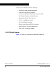
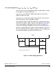
Fast signal transitions on MCU pins place high, short-duration current
demands on the power supply. To prevent noise problems, take special
care to provide power supply bypassing at the MCU as Figure 1-3
shows. Place the bypass capacitors as close to the MCU power pins as
possible. Use high-frequency-response ceramic capacitors for C
BYPASS
.
C
BULK
are optional bulk current bypass capacitors for use in applications
that require the port pins to source high current levels.
Figure 1-3. Power Supply Bypassing
MCU
C
BULK
C
BYPASS
10nF
V
SS1
+
NOTE: Values shown are typical values.
V
DD2
C
BYPASS
10nF
V
DD2
C
BYPASS
10nF
V
SS2
V
SSA
V
DDA
Vbus