
Microcontrollers Data Sheet


Advance Information MC68HC(7)08KH12 — Rev. 1.1
256 Freescale Semiconductor
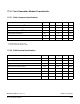
17.13 USB Signaling Levels
17.14 TImer Interface Module Characteristics
Bus State
Signaling Levels
Transmit Receive
Differential 1
D+ > V
OH
(min) and D– < V
OL
(max)
(D+) – (D–) > 200 mV
Differential 0
D– > V
OH
(min) and D– < V
OL
(max)
(D–) – (D+) > 200 mV
Single-ended 0 (SE0)
D+ and D– < V
OL
(max) D+ and D– < V
IL
(max)
(
Data J State
Low Speed
Full Speed
Differential 0
Differential 1
Differential 0
Differential 1
Data K State
Low Speed
Full Speed
Differential 1
Differential 0
Differential 1
Differential 0
Idle State
Low Speed
Full Speed
NA
D– > V
IHZ
(min) and D+ < V
IL
(max)
D+ > V
IHZ
(min) and D– < V
IL
(max)
Resume State Data K State Data K State
Start of Packet (SOP) Data lines switch from Idle to K State
End of Packet (EOP)
SE0 for approximately 2 Bit Times
(1)
Followed by a J for 1 Bit Time
1. The width of EOP is defined in bit times relative to the speed of transmission.
SE0 for ≥ 1 Bit Times
(2)
followed by a J
2. The width of EOP is defined in bit times relative to the device type receiving the EOP. The bit time is approximate.
Reset
D+ and D– < V
OL
(max) for ≥10 ms D+ and D– < V
IL
(max) for ≥ 2.5µs
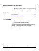
Characteristic Symbol Min Max Unit
Input Capture Pulse Width t
TIH,
t
TIL
125 — ns
Input Clock Pulse Width t
TCH,
t
TCL
(1/f
OP
) + 5 — ns