
Microcontrollers Data Sheet


MC68HC(7)08KH12 — Rev. 1.1 Advance Information
Freescale Semiconductor
253
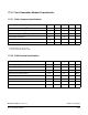
17.10 USB Low Speed Source Electrical Characteristics
Characteristic Symbol
Conditions
(Notes 1,2,3)
Min Typ Max Unit
Transition time:
Rise Time
Fall Time
T
R
T
F
Notes 4, 5, 8
C
L
= 200pF
C
L
=600pF
C
L
=200pF
C
L
=600pF
75
75
—
—
—
300
—
300
ns
Rise/Fall Time Matching T
RFM
T
R
/T
F
80 — 120 %
Output Signal Crossover
Voltage
V
CRS
1.3 — 2.0 V
Low Speed Data Rate T
DRATE
1.5Mbs±1.5%
1.4775
676.8
1.500
666.0
1.5225
656.8
Mbs
ns
Source Differential Driver Jitter
To Next Transition
For Paired Transitions
T
UDJ1
T
UDJ2
C
L
=350pF
Notes 6, 7
–25
–10
—
—
25
10
ns
ns
Receiver Data Jitter Tolerance
To Next Transition
For Paired Transitions
T
DJR1
T
DJR2
C
L
=350pF
Note 7
–75
–45
—
—
75
45
ns
ns
Source EOP Width TEOPT Note 7 1.25 — 1.50 µs
Differential to EOP Transition
Skew
TDEOP Note 7 –40 — 100 ns
Receiver EOP Width
Must Reject as EOP
Must Accept
T
EOPR1
T
EOPR2
Note 7 330
670
—
—
—
—
ns
ns
NOTES:
1. All voltages measured from local ground, unless otherwise specified.
2. All timings use a capacitive load of 50pF, unless otherwise specified.
3. Low speed timings have a 1.5kΩ pull-up to 2.8V on the D– data line.
4. Measured from 10% to 90% of the data signal.
5. The rising and falling edges should be smoothly transitioning (monotonic).
6. Timing differences between the differential data signals.
7. Measured at crossover point of differential data signals.
8. Capacitive loading includes 50pF of tester capacitance.