
Microcontrollers Data Sheet


Advance Information MC68HC(7)08KH12 — Rev. 1.1
250 Freescale Semiconductor
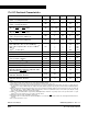
17.6 DC Electrical Characteristics
Characteristic Symbol Min
Typ
(2)
Max Unit
Output High Voltage
(I
LOAD
= –2.0mA) All I/O Pins
V
OH
V
DD
– 0.8 — — V
Output Low Voltage
(I
LOAD
= 1.6mA) All I/O Pins
V
OL
——0.4V
Input High Voltage
All ports, IRQ1
/V
PP
, RST, OSC1
V
IH
0.7 × V
DD
—V
DD
V
Input Low Voltage
All ports, IRQ1
/V
PP
, RST, OSC1
V
IL
V
SS
—0.3 × V
DD
V
Output High Current
(V
OH
= 2.1V) Port C in LDD mode
I
OH
34.56mA
Output Low Current
(V
OL
= 2.3V) Port C in LDD mode
I
OL
10 15 20 mA
V
DD
Supply Current
Run, USB active, PLL on, f
OP
= 6.0MHz
(3)
Run, USB suspended, PLL off, f
OP
= 1.5MHz
(3)
Wait
(4)
Stop
(5)
0°C to 85°C
I
DD
—
—
—
—
—
—
—
—
20
3
1
350
mA
mA
mA
µA
I/O Ports Hi-Z Leakage Current I
IL
——±10 µA
Input Current I
IN
——±1 µA
Capacitance
Ports (as Input or Output)
C
OUT
C
IN
—
—
—
—
12
8
pF
POR ReArm Voltage
(6)
V
POR
0—100mV
POR Rise Time Ramp Rate
(7)
R
POR
0.035 — — V/ms
Monitor Mode Entry Voltage V
DD
+V
HI
1.4 × V
DD
2.0 × V
DD
V
Pullup resistor
PA0-PA7, PB0-PB7, PC0-PC7, PD0-PD7, PE0-
PE3, PF0-PF7, RST
, IRQ1/V
PP
R
PU
20 35 50 kΩ
Schmitt Trigger Input High Level
PD0-PD7, PE0-PE3, PF0-PF7
V
SHI
2.8 3.4 V
Schmitt Trigger Input Low Level
PD0-PD7, PE0-PE3, PF0-PF7
V
SHL
1.7 2.3 V
NOTES:
1. V
DD
= 4.0 to 5.5 Vdc, V
SS
= 0 Vdc, T
A
= T
L
to T
H
, unless otherwise noted.
2. Typical values reflect average measurements at midpoint of voltage range, 25 °C only.
3. Run (operating) I
DD
measured using external square wave clock source. All inputs 0.2 V from rail. No dc loads. Less than 100 pF on
all outputs. C
L
= 20 pF on OSC2. All ports configured as inputs. OSC2 capacitance linearly affects run I
DD
. Measured with all modules
enabled.
4. Wait I
DD
measured using external square wave clock source (f
CGMXCLK
= 6 MHz); all inputs 0.2 V from rail; no dc loads; less than 100
pF on all outputs. C
L
= 20 pF on OSC2; USB in suspend mode, 15 KΩ ± 5% termination resistors on D+ and D– pins; all ports config-
ured as inputs; OSC2 capacitance linearly affects wait I
DD
.
5. STOP I
DD
measured with USB in suspend mode, OSC1 grounded, 1.425 KΩ ± 1% pull-up resistor on D+ pin and 15 KΩ ± 1% pull-
down resistors on D+ and D– pins, no port pins sourcing current.
6. Maximum is highest voltage that POR is guaranteed.
7. If minimum V
DD
is not reached before the internal POR reset is released, RST must be driven low externally until minimum V
DD
is
reached.
8. R
PU
is measured at V
DD
= 5.0V.