
Microcontrollers Data Sheet


Advance Information MC68HC(7)08KH12 — Rev. 1.1
204 Freescale Semiconductor
When bit DDRFx is a logic one, reading address $0009 reads the PTFx
data latch. When bit DDRFx is a logic zero, reading address $0009 reads
the voltage level on the pin. The data latch can always be written,
regardless of the state of its data direction bit. Table 12-7 summarizes
the operation of the port F pins.
12.9 Port Options
All pins of port A, port B and port C have programmable pullup resistors.
Port C also has LED drive capability.
12.9.1 Port Option Control Register (POC)
The pullup option for each port is controlled by one bit in the port option
control register. One bit controls the LED drive configuration on port C.
Table 12-7. Port F Pin Functions
DDRE
Bit
PTE
Bit
I/O Pin Mode
Accesses to
DDRE
Accesses to PTE
Read/Write Read Write
0X
(1)
1. X = don’t care
Input, Hi-Z
(2)
2. Hi-Z = high impedance
DDRF[7:0] Pin PTF[7:0]
(3)
3. Writing affects data register, but does not affect input.
1 X Output DDRF[7:0] PTF[7:0] PTF[7:0]
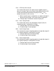
Address: $001D
Bit 7654321Bit 0
Read: 0 0
LDD
00
PCP PBP PAP
Write:
Reset:00100000
= Unimplemented
Figure 12-22. Port Option Control Register (POC)