
Microcontrollers Data Sheet


Advance Information MC68HC(7)08KH12 — Rev. 1.1
196 Freescale Semiconductor
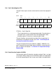
PTE[4:0] — Port E Data Bits
PTE[4:0] are read/write, software-programmable bits. Data direction
of each port E pin is under the control of the corresponding bit in data
direction register E.
TCH1-TCH0 — Timer Channel I/O Bits
The PTE2/TCH1-PTE1/TCH0 pins are the TIM input capture/output
compare pins. The edge/level select bits, ELSxB and ELSxA,
determine whether the PTE2/TCH1–PTE1/TCH0 pins are timer
channel I/O pins or general-purpose I/O pins. See Section 11. Timer
Interface Module (TIM).
NOTE: Data direction register E (DDRE) does not affect the data direction of
port E pins that are being used by the TIM. However, the DDRE bits
always determine whether reading port E returns the states of the
latches or the states of the pins.
TCLK — Timer Clock Input
The PTE0/TCLK pin is the external clock input for the TIM. The
prescaler select bits, PS2-PS0, selects PE0/TCLK as the TIM clock
input. When not selected as the TIM clock, PE0/TCLK is available for
general purpose I/O. See Section 11. Timer Interface Module (TIM).
The PEPE[3:0] bits in the port E keyboard interrupt enable register
enable individual pull-ups on port E pins PTE3–PTE0 if the respective
pin is configured as an input. (See 15.5.3.2 Port-E Keyboard Interrupt
Enable Register.)
The port-E keyboard interrupt enable bits, KBEIE3—KBEIE0, in the port-
E keyboard interrupt enable register (KBEIER), enable the port E pins as
external interrupt pins. See Section 15. Keyboard Interrupt Module
(KBI).
12.7.2 Data Direction Register E (DDRE)
Data direction register E determines whether each port E pin is an input
or an output. Writing a logic one to a DDRE bit enables the output buffer
for the corresponding port E pin; a logic zero disables the output buffer.