
Microcontrollers Data Sheet


Advance Information MC68HC(7)08KH12 — Rev. 1.1
192 Freescale Semiconductor
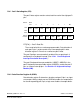
Figure 12-9. Port C I/O Circuit
When bit DDRCx is a logic one, reading address $0002 reads the PTCx
data latch. When bit DDRCx is a logic zero, reading address $0002
reads the voltage level on the pin. The data latch can always be written,
regardless of the state of its data direction bit. Table 12-4 summarizes
the operation of the port C pins.
12.6 Port D
Port D is an 8-bit general-purpose bidirectional I/O port that shares its
pins with the keyboard interrupt module (KBI). All Port D pins have built-
in schmitt triggered input.
Table 12-4. Port C Pin Functions
DDRC
Bit
PTC Bit I/O Pin Mode
Accesses to
DDRC
Accesses to PTC
Read/Write Read Write
0X
(1)
1. X = don’t care
Input, Hi-Z
(2)
2. Hi-Z = high impedance
DDRC[4:0] Pin PTC[4:0]
(3)
3. Writing affects data register, but does not affect input.
1 X Output DDRC[4:0] PTC[4:0] PTC[4:0]
READ DDRC ($0006)
WRITE DDRC ($0006)
RESET
WRITE PTC ($0002)
READ PTC ($0002)
PTCx
DDRCx
PTCx
INTERNAL DATA BUS