
Microcontrollers Data Sheet


Advance Information MC68HC(7)08KH12 — Rev. 1.1
190 Freescale Semiconductor
When bit DDRBx is a logic one, reading address $0001 reads the PTBx
data latch. When bit DDRBx is a logic zero, reading address $0001
reads the voltage level on the pin. The data latch can always be written,
regardless of the state of its data direction bit. Table 12-3 summarizes
the operation of the port B pins.
12.5 Port C
Port C is a 5-bit general-purpose bidirectional I/O port with software
configurable pullups and current drive options.
12.5.1 Port C Data Register (PTC)
The port C data register contains a data latch for each of the five port C
pins.
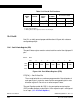
Table 12-3. Port B Pin Functions
DDRB
Bit
PTB Bit I/O Pin Mode
Accesses to
DDRB
Accesses to PTB
Read/Write Read Write
0X
(1)
1. X = don’t care
Input, Hi-Z
(2)
2. Hi-Z = high impedance
DDRB[7:0] Pin PTB[7:0]
(3)
3. Writing affects data register, but does not affect input.
1 X Output DDRB[7:0] PTB[7:0] PTB[7:0]
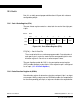
Address: $0002
Bit 7654321Bit 0
Read: 0 0 0
PTC4 PTC3 PTC2 PTC1 PTC0
Write:
Reset: Unaffected by reset
= Unimplemented
Figure 12-7. Port C Data Register (PTC)