
Microcontrollers Data Sheet


MC68HC(7)08KH12 — Rev. 1.1 Advance Information
Freescale Semiconductor
187
DDRA[7:0] — Data Direction Register A Bits
These read/write bits control port A data direction. Reset clears
DDRA[7:0], configuring all port A pins as inputs.
1 = Corresponding port A pin configured as output
0 = Corresponding port A pin configured as input
NOTE: Avoid glitches on port A pins by writing to the port A data register before
changing data direction register A bits from 0 to 1.
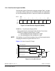
Figure 12-3 shows the port A I/O logic.
Figure 12-3. Port A I/O Circuit
When bit DDRAx is a logic one, reading address $0000 reads the PTAx
data latch. When bit DDRAx is a logic zero, reading address $0000
reads the voltage level on the pin. The data latch can always be written,
regardless of the state of its data direction bit. Table 12-2 summarizes
the operation of the port A pins.
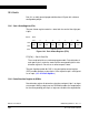
Address: $0004
Bit 7654321Bit 0
Read:
DDRA7 DDRA6 DDRA5 DDRA4 DDRA3 DDRA2 DDRA1 DDRA0
Write:
Reset:00000000
Figure 12-2. Data Direction Register A (DDRA)
READ DDRA ($0004)
WRITE DDRA ($0004)
RESET
WRITE PTA ($0000)
READ PTA ($0000)
PTAx
DDRAx
PTAx
INTERNAL DATA BUS