
Microcontrollers Data Sheet


MC68HC(7)08KH12 — Rev. 1.1 Advance Information
Freescale Semiconductor
181
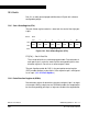
Figure 11-7. CHxMAX Latency
11.9.5 TIM Channel Registers (TCH0H/L–TCH1H/L)
These read/write registers contain the captured TIM counter value of the
input capture function or the output compare value of the output
compare function. The state of the TIM channel registers after reset is
unknown.
In input capture mode (MSxB:MSxA = 0:0), reading the high byte of the
TIM channel x registers (TCHxH) inhibits input captures until the low
byte (TCHxL) is read.
In output compare mode (MSxB:MSxA ≠ 0:0), writing to the high byte of
the TIM channel x registers (TCHxH) inhibits output compares until the
low byte (TCHxL) is written.
OUTPUT
OVERFLOW
PTEx/TCHx
PERIOD
CHxMAX
OVERFLOW OVERFLOW OVERFLOW OVERFLOW
COMPARE
OUTPUT
COMPARE
OUTPUT
COMPARE
OUTPUT
COMPARE