
Microcontrollers Data Sheet


Advance Information MC68HC(7)08KH12 — Rev. 1.1
152 Freescale Semiconductor
10.4.1 Entering Monitor Mode
Table 10-1 shows the pin conditions for entering monitor mode.
If PTC3 is low upon monitor mode entry, CGMOUT is equal to the crystal
frequency. The bus frequency in this case is a divide-by-two of the input
clock. If PTC3 is high upon monitor mode entry, the bus frequency will
be a divide-by-four of the input clock.
NOTE: Holding the PTC3 pin low when entering monitor mode causes a bypass
of a divide-by-two stage at the oscillator. The CGMOUT frequency is
equal to the CGMXCLK frequency, and the OSC1 input directly
generates internal bus clocks. In this case, the OSC1 signal must have
a 50% duty cycle at maximum bus frequency.
Enter monitor mode with the pin configuration shown above by pulling
RST
low and then high. The rising edge of RST latches monitor mode.
Once monitor mode is latched, the values on the specified pins can
change.
Once out of reset, the MCU monitor mode firmware then sends a break
signal (10 consecutive logic zeros) to the host computer, indicating that
it is ready to receive a command. The break signal also provides a timing
reference to allow the host to determine the necessary baud rate.
Monitor mode uses different vectors for reset, SWI, and break interrupt.
The alternate vectors are in the $FE page instead of the $FF page and
allow code execution from the internal monitor firmware instead of user
code.
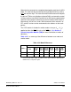
Table 10-1. Mode Selection
IRQ1/V
PP
Pin
PC0 Pin
PC1 Pin
PA0 Pin
PC3 Pin
Mode
CGMOUT
Bus
Frequency
V
DD
+ V
HI
1011Monitor CGMXCLK ÷ 2 CGMOUT ÷ 2
V
DD
+ V
HI
1010Monitor CGMXCLK CGMOUT ÷ 2