
Stereo System - Digital Audio Signal Processor User Manual

ESAI Programming Model
DSP56364 24-Bit Digital Signal Processor Users Manual, Rev. 2
Freescale Semiconductor 6-27
receivers can be enabled) if the input data pin is not used by a transmitter. Operating modes are also
selected in this register.
Hardware and software reset clear all the bits in the RCR register.
The ESAI RCR bits are described in the following paragraphs.
6.3.4.1 RCR ESAI Receiver 0 Enable (RE0) - Bit 0
When RE0 is set and TE5 is cleared, the ESAI receiver 0 is enabled and samples data at the SDO5/SDI0
pin. TX5 and RX0 should not be enabled at the same time (RE0=1 and TE5=1). When RE0 is cleared,
receiver 0 is disabled by inhibiting data transfer into RX0. If this bit is cleared while receiving a data word,
the remainder of the word is shifted in and transferred to the RX0 data register.
If RE0 is set while some of the other receivers are already in operation, the first data word received in RX0
will be invalid and must be discarded.
6.3.4.2 RCR ESAI Receiver 1 Enable (RE1) - Bit 1
When RE1 is set and TE4 is cleared, the ESAI receiver 1 is enabled and samples data at the SDO4/SDI1
pin. TX4 and RX1 should not be enabled at the same time (RE1=1 and TE4=1). When RE1 is cleared,
receiver 1 is disabled by inhibiting data transfer into RX1. If this bit is cleared while receiving a data word,
the remainder of the word is shifted in and transferred to the RX1 data register.
If RE1 is set while some of the other receivers are already in operation, the first data word received in RX1
will be invalid and must be discarded.
6.3.4.3 RCR ESAI Receiver 2 Enable (RE2) - Bit 2
When RE2 is set and TE3 is cleared, the ESAI receiver 2 is enabled and samples data at the SDO3/SDI2
pin. TX3 and RX2 should not be enabled at the same time (RE2=1 and TE3=1). When RE2 is cleared,
receiver 2 is disabled by inhibiting data transfer into RX2. If this bit is cleared while receiving a data word,
the remainder of the word is shifted in and transferred to the RX2 data register.
If RE2 is set while some of the other receivers are already in operation, the first data word received in RX2
will be invalid and must be discarded.
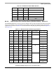
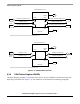
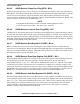
11109876543210
X:$FFFFB7 RSWS1 RSWS0 RMOD RMOD RWA RSHFD
RE3 RE2 RE1 RE0
23 22 21 20 19 18 17 16 15 14 13 12
RLIE RIE REDIE REIE RPR
RFSR RFSL RSWS4 RSWS3 RSWS2
Reserved bit - read as zero; should be written with zero for future compatibility.
Figure 6-9 RCR Register