
User's Manual


FLC-CBM202 Datasheet
Flaircomm Microelectronics Confidential
-5-
TABLES AND FIGURES
Table 1: General Specification ....................................................................................................................................... 11
Table 2: Pin Definition ................................................................................................................................................... 14
Table 3: Analog IO Usage .............................................................................................................................................. 17
Table 4: PCM and I
2
S Digital Audio Interface .............................................................................................................. 21
Table 5: DSSS and CCK modulations (802.11b) TX Performance Specifications ........................................................ 22
Table 6: OFDM TX Performance Specifications ........................................................................................................... 23
Table 7: DSSS and CCK modulations (802.11b) RX Performance Specifications ........................................................ 23
Table 8: OFDM RX Performance Specifications ........................................................................................................... 25
Table 9: Transmitter ....................................................................................................................................................... 26
Table 10: Receiver ......................................................................................................................................................... 26
Table 11: Absolute Maximum Ratings .......................................................................................................................... 27
Table 12: Recommended Operating Conditions ............................................................................................................ 27
Table 13: WiFi Current Consumption ............................................................................................................................ 27
Table 14: BT Current Consumption ............................................................................................................................... 28
Table 15: Digital Characteristics .................................................................................................................................... 28
Table 16: Sleep Clock Characteristics ............................................................................................................................ 28
Table 17: Power-on Reset Characteristics ...................................................................................................................... 29
Table 18: Product Revision ............................................................................................................................................ 35
Table 19: Shipping Package ........................................................................................................................................... 35
Table 20: Product Package ............................................................................................................................................. 35
Table 21: Product Grade ................................................................................................................................................ 36
Table 20: Antenna Electrical Specifications .................................................................................................................. 38
Table 21: Radiation Gain and Pattern ............................................................................................................................ 38
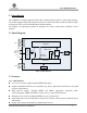
Figure 1: Block Diagram .................................................................................................................................................. 6
Figure 2: Pin Configuration............................................................................................................................................ 12
Figure 3: UART_TX Timing ......................................................................................................................................... 19
Figure 4: PCM Interface Master ..................................................................................................................................... 20
Figure 5: PCM Interface Slave ....................................................................................................................................... 20
Figure 6: Reference Design ............................................................................................................................................ 30
Figure 7: Module Size (Top View and Side View) ........................................................................................................ 31
Figure 8: Footprint (Top View) ...................................................................................................................................... 31
Figure 9: Pin dimensions ................................................................................................................................................ 31
Figure 10: Placement the Module on a System Board ................................................................................................... 32
Figure 11: Leave 5mm Clearance Space from the Antenna ........................................................................................... 32
Figure 12: Recommended Trace Connects Antenna and the Module ............................................................................ 33
Figure 13: Recommended Reflow Profile ...................................................................................................................... 34
Figure 14: Product Packaging Information .................................................................................................................... 35
Figure 15: Ordering Information .................................................................................................................................... 35
Figure 12: ALA931C5 Radiation Pattern : Azimuth@2.45GHz .................................................................................... 39
Figure 13: ALA931C5 Radiation Pattern : Elevation1@2.45GHz ............................................................................... 40
Figure 14: ALA931C5 Radiation Pattern : Elevation2@2.45GHz ............................................................................... 41