
User's Manual

FLC-CBM202 Datasheet
Flaircomm Microelectronics Confidential
-28-
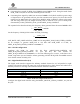
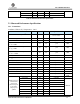
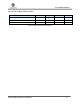
5.3.3.2 BT Current Consumption
State
Min
Typical
Max
Unit
Continuous receive
-
TBD
-
mA
Continuous transmit
-
TBD
-
mA
Leakage(deep sleep, including internal sleep clock )
-
TBD
-
μA
Table 14: BT Current Consumption
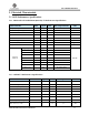
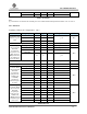
5.3.4 Digital Characteristics
Digital Terminals
Min
Typical
Max
Unit
Input Voltage Levels
VIL input logic level low
-0.3
-
0.25VDD
V
VIH input logic level high
0.625VDD
-
VDD+0.3
V
Output Voltage Levels
VOL output logic Level low, IOL=8.0mA
-
-
0.4
V
VOH output logic Level high, IOH=-8.0mA
0.75VDD
-
VDD
V
Input and Tri-state Currents
Strong pull-up
-150
-40
-10
μA
Strong pull-down
10
40
150
μA
Weak pull-up
-5
-1.0
-0.33
μA
Weak pull-down
0.33
1.0
5.0
μA
CI Input Capacitance
1.0
-
5.0
pF
Table 15: Digital Characteristics
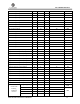
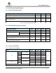
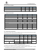
5.3.5 Sleep Clock Characteristics
Sleep clock is an option with external 32.768 KHz clock for deep sleep and other low-power modes.
Following table lists the requirements for the sleep clock.
Sleep Clock
Min
Typical
Max
Unit
Frequency(a)
30
32.768
35
kHz
Frequency tolerance(b)
-
-
±250
ppm
Duty cycle
5:95
50:50
95:5
%
Jitter
Integrated rms jitter 10Hz to 20kHz
f
ref
=32.768kHz
-
-
20
ns rms
Phase noise
f
ref
=32.768kHz
1kHz offset
-
-
-100
dBc/Hz
10kHz offset
-
-
-120
Table 16: Sleep Clock Characteristics
(a) Stability is most important as frequency is calibrated against the system clock.
(b) The frequency of the slow clock is periodically calibrated against the system clock, as a result
the frequency is more important than the maximum deviation.