
User's Manual

FLC-CBM202 Datasheet
Flaircomm Microelectronics Confidential
-16-
4.3.1 WiFi reset
Via the external RST# pin (pin 5)
Via an internal core power supply supervisor
Using software watchdog timers
Via SDIO/CSPI host interface
RST# is an active-low reset input that is internally filtered using the internal low frequency clock
oscillator to avoid spurious resets. A reset occurs after the signal has been asserted for between 250
and 375 s. This pin may be tied to WIFI_VDDIO if unused; otherwise it should be asserted for at
least 1 ms to force a reset.
The power supply monitors WIFI_VDD_DIG to trigger a power-on-reset. This occurs when the
supply falls below 1.05V (typical) in normal operation or 0.785 V (typical) in deep sleep, and ends
when the supply exceeds 1.10V (typical). Glitches of up to 30mV and 2.5s duration, which could
be caused by large load steps, will not trigger a reset.
Each of the internal processors has its own independent watchdog timer to detect and recover from
erroneous software operation. These are typically configured with a timeout of 1.5s, but this may be
increased up to maximum of 64s for reduced power consumption. The watchdogs are enabled at
power-on and continue operating while FLC-CBM202 is in deep sleep.
4.3.2 BT Reset
The BT reset function is internally tied to the BT_nRESET pin. The BT may be reset from several
sources:
BT_nRESET pin
Power-on reset
A UART break character
Via a software-configured watchdog timer
The BT_nRESET pin is an active low reset. To ensure a full reset the reset signal should be asserted
for a period greater than 5ms.
A warm reset function is also available under software control. After a warm reset the RAM data
remains available.
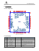
4.4 RF Interface
Pin 1 is the RF port used for WiFi and BT to receive and transmit. A shared antenna algorithm is
adopted. A 50 antenna can be directly connected to this port (Pin 1). However, a п matching
circuit is recommended to match an antenna to this RF port.