FLC-CBM202 Datasheet FLC-CBM202 Datasheet Document Type: Combo Module Datasheet Document Number: FLC-CBM202-DS Document Version: V1.2 Release Date: Feb.22, 2013 Copyright 2012 ~ 2014 by Flaircomm Microelectronics, Inc., All Right Reserved Without written permission from Flaircomm Microelectronics, Inc.
FLC-CBM202 Datasheet Release Record Version Release Date 0.1 0.2 1.0 1.1 1.2 June 16, 2011 August 05, 2011 July 3, 2012 Jan. 11, 2013 Feb.22,2013 Flaircomm Microelectronics Confidential Comments Preliminary Release Add Section5.2 Add Section 11 Modify Frequency Band.
FLC-CBM202 Datasheet CONTENTS 1. INTRODUCTION .................................................................................................................................................. 6 1.1 BLOCK DIAGRAM .................................................................................................................................................. 6 1.2 FEATURES ......................................................................................................................................
FLC-CBM202 Datasheet 8.1 9. 10. ANTENNA CONNECTION AND GROUNDING PLANE DESIGN ................................................................................. 32 RECOMMENDED REFLOW PROFILE ......................................................................................................... 34 ORDERING INFORMATION ....................................................................................................................... 35 10.1 PRODUCT PACKAGING INFORMATION ................................
FLC-CBM202 Datasheet TABLES AND FIGURES Table 1: General Specification ....................................................................................................................................... 11 Table 2: Pin Definition ................................................................................................................................................... 14 Table 3: Analog IO Usage .....................................................................................................
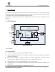
FLC-CBM202 Datasheet 1. Introduction FLC-CBM202 is a highly integrated module that combines WiFi and BT in a small single package. The module supports SDIO and CSPI host interfaces for WiFi and UART for BT that make it simple to design into fully certified embedded WiFi and BT solutions. The module is an appropriate product for designers who want to add wireless capability to their products. 1.
FLC-CBM202 Datasheet Internal WEP engine allows 64 or 128 bit Encryption with Temporal Key Integrity Protocol (TKIP) Hardware encryption support for WEP40/64, WEP 104/128, TKIP, CCMP (AES), BIP and CKIP provides functionality for WPA, WPA2, IEEE802.11i, 802.11w and CCX advanced security mechanisms. Module support WAPI security in China also. Support 802.11e Quality of Service (QoS) with WMM Power Save ensures that mobile solutions can achieve optimal battery life.
FLC-CBM202 Datasheet MAC Comprehensive MAC functionality according to IEEE 802.11-2007, including QoS traffic scheduling; Support the following optional IEEE802.11n features; MPDU aggregation MSDU aggregation Immediate Block Acknowledgement PSMP MTBA RIFS L-SIG TXOP protection Link adaptation using MCS feedback Encryption Hardware encryption according to IEEE 802.11-2007 and IEEE802.
FLC-CBM202 Datasheet Physical Interfaces UART BCSP, H4, H4DS and H5 support PCM/I2S interface Synchronous serial interface up to 4Mbps for system debugging 1.
FLC-CBM202 Datasheet 2. General Specification WiFi Specification Standard Frequency Range IEEE 802.11b/g/n FCC : 2.412GHz-2.462GHz CE :2.422GHz -2.472GHz Maximum Data Rate 72.2Mbps RF Input Impedance 50 ohms Interface SDIO / SPI Sensitivity Refer to 5.1 RF TX Power Refer to 5.1 Encryption WEP40/64/104/128, CCMP(AES), TKIP, BIP, WAPI Bluetooth Specification Standard Frequency Band BT 3.0 / BT 4.0 2.402GHz ~ 2.
FLC-CBM202 Datasheet Certifications Environmental WiFi Alliance/FCC/CE RoHS Compliant Dimension and Weight Dimension Weight 9.9mm x 9.9mm x1.
FLC-CBM202 Datasheet 3. Pin Definition 3.1 Pin Configuration Figure 2: Pin Configuration 3.2 Pin Definition Pin Symbol I/O Type 1 ANTENNA A Antenna for BT&WIFI 2 GND P Ground 3 BT_VDD_AUX P 4 BT_VDD_RF P 5 BT_VDDIO P Power in for BT IO 6 BT_SLEEP_CLK IO an external 32.768khz clock is required for BT’s sleep mode Flaircomm Microelectronics Confidential Description Power out for BT_AUX Need a 470nF decouple capacitor on this pin Power out for BT_RADIO/ANA Need a 2.
FLC-CBM202 Datasheet 7 BT_PCM2_OUT IO The PCM data out from BT 8 BT_PCM2_IN IO The PCM data in to BT 9 BT_PCM2_CLK IO The PCM CLK signal 10 BT_PCM2_SYNC IO The PCM SYNC signal 11 BT_SPI_PCM#_SEL IO SPI mode is Active high PCM mode is Active low 12 TCXO1.8V P Power in for internal TCXO 13 BT_WAKEUP IO A wakeup signal from BT to host 14 BT_nRESET IO Reset pin for BT(Active low) 15 BT_1.8V P Power in for BT 16 BT_VDD_DIG P Power out for BT_DIG Need a 2.
FLC-CBM202 Datasheet 36 WIFI_SD_DATA2 IO WIFI SDIO DATA2 37 WIFI_VDDRF3.
FLC-CBM202 Datasheet 4. Physical Interfaces 4.1 WiFi Power Supply 4.1.1 Linear Regulator for Digital Supply A 1.2V LDO in CBM202 powers the core digital circuits and WiFi_VREG_IN_DIG1.8V(Pin17) is the input voltage. The range of this voltage is from 1.45V to 2.0V. WiFi_VDD_DIG (Pin19) is the output of this LDO. A low ESR 2.2uF and a 10nF capacitors to ground should be connected to this pin. 4.1.2 Linear Regulator for Analogue Supply Three 1.
FLC-CBM202 Datasheet 4.3.1 WiFi reset Via the external RST# pin (pin 5) Via an internal core power supply supervisor Using software watchdog timers Via SDIO/CSPI host interface RST# is an active-low reset input that is internally filtered using the internal low frequency clock oscillator to avoid spurious resets. A reset occurs after the signal has been asserted for between 250 and 375 s.
FLC-CBM202 Datasheet 4.5 Host Interface 4.5.1 WiFi Host Interfaces The WiFi of FLC-CBM202 has a single host interface port that can be configured into one of four modes: SD 1-bit SD 4-bit SDIO SPI CSPI The first three modes operate according to the SD Card specifications. The fourth mode is a CSR proprietary variant designed to allow more efficient implementation on hosts without dedicated SDIO host controller. Table 3 shows the usage of the host interfaces pins in each mode.
FLC-CBM202 Datasheet 4.5.1.1.1 SDIO Sleep Signaling FLC-CBM202 supports a variety of mechanisms to enable both itself and the host to efficiently enter and leave low-power modes. 4.5.1.1.1.1 Card Sleep and Wake-up FLC-CBM202 automatically uses its sleep modes to minimize power consumption. Registers in function 0 are always directly accessible by the host, irrespective of the device’s sleep modes. Attempts to access function 1 while the device is in deep sleep are likely to results in SDIO timeouts.
FLC-CBM202 Datasheet The same pin assignments are used for both SD SPI and CSPI as summarized in Table 4. Both the SDIO protocols and CSPI provide access to the same functions and registers within the device; the only difference is with the format of the commands used to perform these accesses. 4.5.2 Bluetooth UART Host Interfaces CBM202 BT UART interface provides a simple mechanism for communicating with other serial devices using the RS-232 protocol.
FLC-CBM202 Datasheet Hardware on the CBM202 for sending data to and from a SCO connection. Up to 3 SCO connections on the PCM interface at any one time. PCM interface master, generating PCM_SYNC and PCM_CLK. PCM interface slave, accepting externally generated PCM_SYNC and PCM_CLK. Various clock formats including: Long Frame Sync Short Frame Sync GCI timing environments 13-bit or 16-bit linear, 8-bit μ-law or A-law commanded sample formats.
FLC-CBM202 Datasheet Generating these signals by DDS from CBM202 internal 4MHz clock. Using this mode limits PCM_CLK to 128, 256 or 512 kHz and PCM_SYNC to 8 kHz. Generating these signals by DDS from an internal 48MHz clock (which enables a greater range of frequencies to be generated with low jitter but consumes more power). To select this second method set bit 48M_PCM_CLK_GEN_EN in PSKEY_PCM_CONFIG32.
FLC-CBM202 Datasheet 5. Electrical Characteristic 5.1 WiFi Performance Specifications 5.1.1 DSSS and CCK modulations (802.11b) TX Performance Specifications Characteristics Min Typical Max IEEE Specification Unit Frequency range 2400 - 2500 - MHz RMS transmit power(a) 16 18 20 - dBm RMS EVM 0 -28 -25 -9.
FLC-CBM202 Datasheet Spectral flatness for spectral lines -26 to -17,17 to 26 - - -4 to 2 -4 to 2 Frequency(GHz) Min Typical Max 0.076-0.108 - -160 - 0.776-0.794 - -145 - 0.869-0.894 - -145 - 0.925-0.960 - -143 - 1.570-1.580 - -135 - 1.805-1.880 - -132 - 1.930-1.990 - -130 - 2.110-2.170 - -125 - Spurious emissions dB dBm/Hz Table 6: OFDM TX Performance Specifications 5.1.3 DSSS and CCK modulations (802.
FLC-CBM202 Datasheet Rx sensitivity,6Mbps - -92 -84 -82 dBm Rx sensitivity,9Mbps - -91 -82 -81 dBm Rx sensitivity,12Mbps - -90 -82 -79 dBm Rx sensitivity,18Mbps - -87 -78 -77 dBm Rx sensitivity,24Mbps - -84 -76 -74 dBm Rx sensitivity,36Mbps - -81 -73 -70 dBm Rx sensitivity,48Mbps - -75 -69 -66 dBm Rx sensitivity,54Mbps - -74 -68 -65 dBm Rx sensitivity,MCS0 - -92 -84 -82 dBm Rx sensitivity, MCS1 - -89 -81 -79 dBm Rx sensitivity, MCS2 - -87 -78 -
FLC-CBM202 Datasheet 1.710-1.785 - 1 - GSM1800/DCS1800 1.850-1.910 - 0 - GSM1900/PCS1900 1.920-1.980 - -3 - W-CDMA 2000 Table 8: OFDM RX Performance Specifications 5.2 Bluetooth Performance Specifications 5.2.1 Transmitter Condition: VDD=1.8V, Temperature= +20°C.
FLC-CBM202 Datasheet 2.110-2.170 - -136 - W-CDMA 2000 2.110-2.170 - -136 - W-CDMA 2000 Table 9: Transmitter Note: (a) The firmware can maintain the transmit power to be within the Bluetooth specification limits: class 1 or class 2. 5.2.2 Receiver Condition: VDD=1.8V, Temperature= +20°C. Frequency Min Typical Max 2.402 - -86.0 - 2.441 - -86.0 - 2.480 - -86.0 - Maximum received signal at 1.
FLC-CBM202 Datasheet 5.3 DC Electrical Specifications 5.3.1 Absolute Maximum Ratings Rating Min Max Unit -40 +85 °C Linear regulator voltage 1.8V +1.45 +2.0 V I/O supply voltage(VDD_SDIO, VDD_PADS_PIO_0_7, VDD_AIO_PIO_8_15) +1.7 +3.6 V VSS-0.3 VDD+0.3 V Min Typical Max Unit -40 - +85 °C for A and I grade -40 - +85 °C for V and C grade -20 - +70 °C 1.7 - 3.6 V 1.7 - 3.3 V 1.75 - 1.
FLC-CBM202 Datasheet 5.3.3.2 BT Current Consumption State Min Typical Max Unit Continuous receive - TBD - mA Continuous transmit - TBD - mA Leakage(deep sleep, including internal sleep clock ) - TBD - μA Table 14: BT Current Consumption 5.3.4 Digital Characteristics Digital Terminals Min Typical Max Unit VIL input logic level low -0.3 - 0.25VDD V VIH input logic level high 0.625VDD - VDD+0.3 V - - 0.4 V 0.
FLC-CBM202 Datasheet 5.3.6 Power-on Reset Characteristics Power-on Reset Min Typical Max Unit Reset release on VDD_DIG rising(HL) 1.030 - 1.150 V Reset assert on VDD_DIG falling(LO) HL-0.060 - HL-0.045 V 0.770 0.785 0.
L11 L9 BT1.8V L8 C6 2.2uF C5 100nF WIFI_SDIO3.3V C16 1uF WIFI POWER L2 TBD 10K WIFI3.3V R3 BT1.8V 2.2uF C2 R1 10K TCXO1.8 BLM15AG121SN1 L3 BLM15AG121SN1 WIFI_VDDAIO_3V3 C14 L4 470nF 2.2uF BT_VDD_IO 2.2uF 470nF WIFI_VDD_RF_3V3 C15 NC C3 C4 49 12 11 10 9 8 7 6 5 4 3 2 1 WIFI1.8V GND3 TCXO1.
FLC-CBM202 Datasheet 7.
FLC-CBM202 Datasheet 8. Recommended PCB Layout and Mounting Pattern Placement and PCB layout are critical to optimize the performances of a module without on-board antenna designs. The trace from the antenna port of the module to an external antenna should be 50 and must be as short as possible to avoid any interference into the transceiver of the module. The location of the external antenna and RF-IN port of the module should be kept away from any noise sources and digital traces.
FLC-CBM202 Datasheet Distance between connection and ground area on the top layer should at least be as large as the dielectric thickness. Routing the RF close to digital sections of the system board should be avoided. To reduce signal reflections, sharp angles in the routing of the micro strip line should be avoided. Chamfers or fillets are preferred for rectangular routing; 45-degree routing is preferred over Manhattan style 90-degree routing.
FLC-CBM202 Datasheet 9. Recommended Reflow Profile The soldering profile depends on various parameters necessitating a set up for each application. The data here is given only for guidance on solder reflow. ℃ 250 217 210 A 25 0 B 1 2 C 3 D 4 E 5 6 min Figure 13: Recommended Reflow Profile Pre-heat zone (A) — This zone raises the temperature at a controlled rate, typically 0.5 – 2 C/s. The purpose of this zone is to preheat the PCB board and components to 120 ~ 150 C.
FLC-CBM202 Datasheet 10. Ordering Information 10.1 Product Packaging Information TBD Figure 14: Product Packaging Information 10.2 Ordering information FLC-CBM202CL2A Product Revision Shipping Package Product Package Product Grade Figure 15: Ordering Information 10.2.1 Product Revision Product Revision Description Availability A Release A Yes Table 18: Product Revision 10.2.
FLC-CBM202 Datasheet 10.2.
FLC-CBM202 Datasheet 11. Cautions &Warnings 11.1 FCC Statement 1. This device complies with Part 15 of the FCC Rules. Operation is subject to the following two conditions: (1) This device may not cause harmful interference. (2) This device must accept any interference received, including interference that may cause undesired operation. 2. Changes or modifications not expressly approved by the party responsible for compliance could void the user's authority to operate the equipment.
FLC-CBM202 Datasheet The packaging of host system that uses CBM202 should display a label indicating the information as follows: Contains FCC ID: P4ICBM202 Model: FLC-CBM202CL2A/FLC-CBM202IL2A/FLC-CBM202VL2A Any similar wording that expresses the same meaning may also be used. 11.4 FLC-CBM202 Antenna Statement 11.4.1 Antenna Electrical Specifications Part Number Frequency Range (GHz) Temperature Average Gain VSWR Impedance ALA931C5 2.4~ 2.485 21.5°C typ. -3 dBi min. 2.5:1 max.
FLC-CBM202 Datasheet Figure 16: ALA931C5 Radiation Pattern : Azimuth@2.
FLC-CBM202 Datasheet Figure 17: ALA931C5 Radiation Pattern : Elevation1@2.
FLC-CBM202 Datasheet Figure 18: ALA931C5 Radiation Pattern : Elevation2@2.