
Hardware Guide

Reproduction forbidden without Fibocom Wireless Inc. written authorization - All rights reserved.
FIBOCOM MC610 Series Hardware Guide 50/71
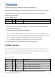
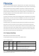
Pin name
I/O
Pin
Description
CSI_D0P
I/O
89
CAMERA MIPI data D0 positive terminal;
CAM_SCK SPI CAM serial clock signal
CSI_CKN
O
92
CAMERA MIPI clock CLK negative terminal;
CAM_RSTL SPI CAM reset signal
CSI_CKP
O
91
CAMERA MIPI clock CLK positive terminal;
CAM_SI0 SPI CAM serial data signal 0
I2C_SDA0
I/O
52
CAMERA I2C data signal
I2C_SCL0
O
56
CAMERA I2C clock signal
For the detailed design of CAMERA, see the latest MC610 Series Reference Design.
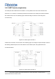
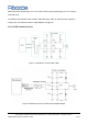
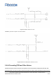
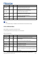
3.12 LCD Interface
MC610 OPEN can support SPI LCD interface screen.
The following table shows the pin description of the LCD interface:
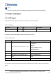
Table 3-19 LCD interface
Pin name
I/O
Pin
Description
LCD_SDC*
I/O
62
LCD command and data switching control signal
LCD_RSTB*
O
74
LCD reset signal
This pin cannot be reused as GPIO function
LCD_CS*
O
69
LCD chip selection signal
LCD_CLK*
O
54
Clock signal line of LCD SPI
LCD_SIO*
I/O
58
Data signal line of LCD SPI
SINK1
I
97
Current source input pin, connected to the cathode of the
backlight, by adjusting the current to adjust the brightness of
the backlight.
Note: