
Hardware Guide


Reproduction forbidden without Fibocom Wireless Inc. written authorization - All rights reserved.
FIBOCOM MC610 Series Hardware Guide 36/71
Pin Name
I/O
Pin
Description
VBUS_IN/VBUS
PI
31,113
USB insertion detection
For more information about the USB Specification 2.0, visit http://www.usb.org/home.
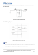
Since the module supports USB 2.0 High-Speed, the equivalent capacitance of the TVS tube on
the USB_DM/DP differential signal line is required to be less than 1 pF, and TVS with capacitance
of 0.5 pF is recommended;
It is recommended to connect serial 0 Ω resistors on the USB_DM/DP differential line;
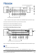
USB_DM and USB_DP are high-speed differential signal lines with a maximum transmission rate
of 480 Mbits/s. PCB Layout must observe the following rules:
⚫ The control differential impedance of USB_DM and USB_DPUSB_DP signal lines is 90 Ω;
⚫ USB_DM and USB_DP signal lines are required to be equal in length and parallel to avoid
right-angle route;
⚫ USB_DM and USB_DP signal lines are laid in the signal layer nearest to the ground, and
protected by surrounding grounding lines in all directions of the line.
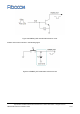
3.5 USIM Interface
MC610 series modules support USIM interfaces, 1.8 V and 3.0 V SIM cards.
3.5.1 USIM Pins
USIM pins are shown in the following table:
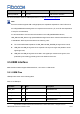
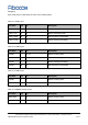
Table 3-10 USIM pins
Pin Name
I/O
Pin
Description
SIM1_SIO
I/O
23
USIM/SIM1DATA
SIM1_CLK
O
24
USIM/SIM1 Clock Signal
SIM1_RST
O
25
USIM/SIM1 RESET Signal
VSIM1
PO
26
USIM/SIM1Power
Note: