
Hardware Guide

Reproduction forbidden without Fibocom Wireless Inc. written authorization - All rights reserved.
FIBOCOM MC610 Series Hardware Guide 25/71
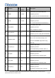
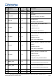
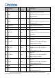
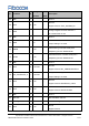
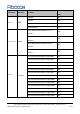
Pin
Pin Name
I/O
Voltage
Domain
Reset
Value
Description
LCD_FMARK/GPIO/FLS1SIO3/U2TXD
125
GND
G
-
-
Ground
126
GPIO
I/O
1.8V
L
GPIO14
Support function SCL2/GPIO
127
GPIO
I/O
1.8V
L
GPIO15
Support function SDA2/GPIO
128
GND
G
-
-
Ground
⚫ Unused pins are keep floating,”*” mean in development.
⚫ A single KEYIN/OUT key cannot be used, and it needs to be used with KEYOUT/IN.
⚫ When USB_BOOT/KEY_IN0 pin and KEYOUT are used as key function in combination, if the
corresponding key is pressed during power-on, the module will enter download mode
because KEYOUT has high pulse output during power-on.
⚫ 3V* in the above table indicates that the pin supports 3 V voltage domain, but the software
configuration needs to be changed in the OPEN version.
⚫ RESET_N and EMERG_RST Pin definitions are the same.
⚫ VBUS and VBUS_IN Pin definitions are the same.
⚫ BT/WIFI-SCAN This function is supported by only some models.
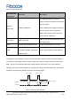
⚫ PWT* is a PWM waveform whose frequency and duty cycle are adjustable.
⚫ PWL* Outputs an unfixed waveform.
⚫ SIM2_SIO*/SIM2_SCLK*/SIM2_SRST*/VSIM2* The SIM2 function has been implemented,
but the dual-card function depends on the software version.
3.1.3 Pin Multiplexing
⚫ The above pin definition only represents the default definition in the standard version. For other
function multiplexing requirements, see FIBOCOM MC610 GPIO Function Multiplexing.
Note: