
Hardware Guide

Reproduction forbidden without Fibocom Wireless Inc. written authorization - All rights reserved.
FIBOCOM MC610 Series Hardware Guide 22/71
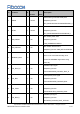
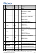
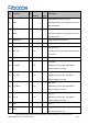
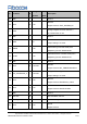
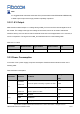
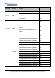
Pin
Pin Name
I/O
Voltage
Domain
Reset
Value
Description
86
GND
G
-
-
Ground
87
KEY_OUT3
O
1.8V
-
KEYOUT3
KEYOUT cannot be used alone.
88
KEY_IN3
I
1.8V
-
Key pad input 3
KEYIN cannot be used alone.
89
CSI_D0P
I/O
1.8V
-
MIPICSI_DATA_P0, CAM MIPI data 0
positive terminal
Multiplexing function
CAM_SCK/CSI_D0P/GPIO23
90
CSI_D0N
I/O
1.8V
-
MIPICSI_DATA_N0, CAM MIPI data 0
negative terminal
Multiplexing function
CAM_SI1/CSI_D0N/GPIO22
91
CSI_CKP
O
1.8V
-
MIPICSI_CLOCK_P, CAM MIPI clock positive
terminal
Multiplexing function
CAM_SI0/CSI_CKP/GPIO21
92
CSI_CKN
O
1.8V
-
MIPICSI_CLOCK_N, CAM MIPI clock
negative terminal
Multiplexing function
CAM_RSTL/CSI_CKN/GPIO18/SCL1
93
DEBUG_TXD
O
1.8V
-
DEBUG serial port transmission
It is recommended to reserve test points
94
DEBUG_RXD
I
1.8V
-
DEBUG serial port receiving
It is recommended to reserve test points
95
VSIM2
PO
1.8/3.0V
-
SIM2 supply output
96
NC