
Hardware Guide


4 Circuit Design
Copyright © Fibocom Wireless Inc. 61
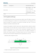
Figure 29. Two-layer PCB coplanar waveguide structure
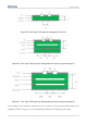
Figure 30. Four-layer PCB coplanar waveguide structure (see ground layer 3)
Figure 31. Four-layer PCB coplanar waveguide structure (see ground layer 4)
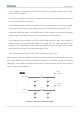
In the design of RF antenna interface circuit, in order to ensure good performance and
reliability of the RF signal, it is recommended to observe the following principles: