
Hardware Guide


4 Circuit Design
Copyright © Fibocom Wireless Inc. 60
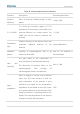
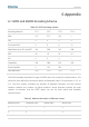
Indicator
Description
Recommended Value
Input power
- -
Peak power >33 dBm
(2 W) in GSM system
Average power >23 dBm
in WCDMA<E systems
VSWR
- -
≤ 2:1
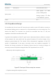
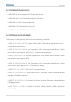
4.5.2 Impedance Design
For modules that do not have a RF connector, you need to route a RF cable to connect to
the antenna feeding point or connector. It is recommended to use a microstrip line. The
shorter the better. The insertion loss should be controlled less than 0.2 dB, and
impedance should be controlled within 50Ω.
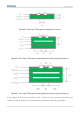
In general, the impedance of the RF signal route is determined by the dielectric constant
of the material, the route width (W), the ground clearance (S) and the height of the
reference ground plane (H). The control of the characteristic impedance of the PCB
usually is implemented in two ways: microstrip route and coplanar waveguide. To
illustrate the design principles, the following figures show the structural designs of
microstrip route and coplanar waveguide when the impedance line is at 50Ω.
Microstrip cable complete structure
Figure 28. Two-layer PCB microstrip line structure
Coplanar waveguide complete structure