
Hardware Guide

4 Circuit Design
Copyright © Fibocom Wireless Inc. 48
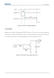
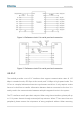
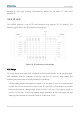
The SD signal line must be grounded all around and kept away from RF antenna,
DCDC power supply, clock signal line and other strong interference sources.
Reference ground must be installed for the SD signal line, and data line impedance
must be controlled with 50 Ω (±10%).
It is recommended to install resistors between the module and SD card connector in
serial mode, and reserve bypass capacitors C1 to C6. In case of interference or ESD
issue, you can adjust the capacitors and resistors to improve signal quality.
The capacitance on the SD signal line must be smaller than 40 pF.
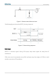
4.4.5 ADC
The module provides three analog-to-digital conversion interfaces. Run the
AT+MMAD="0/1" command to read the voltage value of ADC interface. The voltage range
of ADC interface is 0 V–1.8 V.
To improve the accuracy of ADC voltage measurement, it is recommended
that the ADC be grounded during wiring.
4.4.6 USIM
The module has a built-in (U)SIM card interface, and supports 1.8 V and 3.0 V (U)SIM card.
4.4.6.1 (U)SIM Card Connector with Card Detection Signal
During (U)SIM design, you must select a (U)SIM card connector. A hot plugging card
connector (recommended model: SIM016-8P-220P) with (U)SIM card detection function is
recommended.