
Hardware Guide

4 Circuit Design
Copyright © Fibocom Wireless Inc. 40
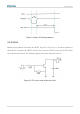
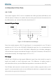
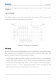
Figure 11. Button reset reference circuit
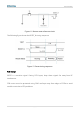
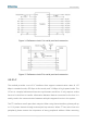
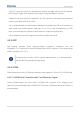
The following figure shows the RESET_N timing sequence.
Figure 12. Reset timing sequence
PCB Design
RESET is a sensitive signal. During PCB layout, keep these signals far away from RF
interference.
PCB routes must be protected using GND and kept away from edges of PCBs to avoid
module reset due to ESD problems.