
Hardware Guide

3 Pins
Copyright © Fibocom Wireless Inc. 32
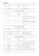
Pin No.
Pin Name
I/O
Power
domain
Description
positive signal, close to PHY string 0.1
uF capacitor
116
SGMII_MDATA
IO
1.8/2.85 V
SGMII data, 1.8/2.85 V power domain.
It needs to be externally pulled up to
VDD_AUX with a 1.5 kΩ pull-up
resistor.
117
SGMII_MCLK
DO
1.8/2.85 V
SGMII clock
44
VDD_AUX
PO
1.8/2.85 V
SGMII_MDATA pull-up power supply,
output of 1.8/2.85 V, configurable
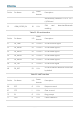
Table 36. LCD interface
Pin No.
Pin Name
I/O
Power
domain
Description
94
LCD_D0
IO
1.8 V
LCD bus data bit 0
8
LCD_D1
IO
1.8 V
LCD bus data bit 1
93
LCD_D2
IO
1.8 V
LCD bus data bit 2
7
LCD_D3
IO
1.8 V
LCD bus data bit 3
88
LCD_D4
IO
1.8 V
LCD bus data bit 4
89
LCD_D5
IO
1.8 V
LCD bus data bit 5
90
LCD_D6
IO
1.8 V
LCD bus data bit 6
120
LCD_D7
IO
1.8 V
LCD bus data bit 7
73
PCM_OUT/LCD_D8
DO
1.8 V
PCM data output/LCD bus data bit 4
72
DTR/LCD_NRST
DI
1.8 V
Sleep mode control/LCD bus reset
signal