
Hardware Guide

3 Pins
Copyright © Fibocom Wireless Inc. 26
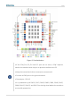
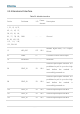
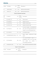
Table 23. PCM interface
Pin No.
Pin Name
I/O
Power
domain
Description
73
PCM_OUT/LCD_D8
DO
1.8 V
PCM data output/LCD bus data bit 4
74
PCM_IN
I
1.8 V
PCM data Input
75
PCM_SYNC/LCD_TE
IO
1.8 V
PCM synchronization signal/LCD bus data
synchronization
76
PCM_CLK/LCD_NCS
IO
1.8 V
PCM clock signal/LCD bus chip select
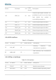
Table 24. USB interface
Pin No.
Pin Name
I/O
Power
domain
Description
11
USB_VBUS
AI
- -
USB insertion detection, typical value: 5 V
12
USB_DN
IO
- -
USB differential data signal (-)
13
USB_DP
IO
- -
USB differential data signal (+)
16
USB_ID
- -
- -
Primary and secondary USB bus
identification, only applicable to the OTG
function
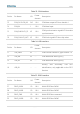
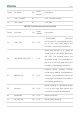
Table 25. SDIO interface
Pin No.
Pin Name
I/O
Power
domain
Description
27
SDIO_DATA1
IO
1.8 V
WLAN SDIO bus DATA1
28
SDIO_DATA2
IO
1.8 V
WLAN SDIO bus DATA2
29
SDIO_CMD
IO
1.8 V
WLAN SDIO bus command
30
SDIO_DATA0
IO
1.8 V
WLAN SDIO bus DATA0