
Datasheet


© 2011 Fairchild Semiconductor Corporation www.fairchildsemi.com
FSA8049 • Rev. 1.0.2 4
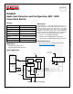
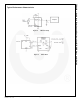
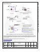
FSA8049 — Audio Jack Detection and Configuration, MIC/GND Cross point Switch
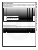
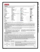
DC Electrical Characteristics
All typical values are at T
A
=25°C unless otherwise specified.
Symbol Parameter V
DD
(V) Condition
T
A
=-40 to +85°C
Unit
Min. Typ. Max.
MIC Switch (MIC to (GND/MIC1 or GND/MIC2))
R
ON(MIC)
MIC Switch On Resistance
2.8
I
OUT
=24 mA, V
IN
=1.8 V
3.00 5.00
Ω
3.8 2.50 4.00
R
FLAT(ON)
On Resistance Flatness
2.8
I
OUT
=24 mA, V
IN
=1 V to V
DD
0.25 0.50
Ω
3.8 0.20 0.40
V
IN(MIC)
Switch Input Voltage Range
2.7 to 4.4
0 V
DD
V
C
ON(MIC)
MIC Switch On Capacitance
(3)
3.8 f=1 MHz 90 pF
C
OFF(MIC)
MIC Switch Off Capacitance
(3)
3.8
f=1 MHz
21 pF
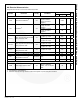
GND Switch (GND to (GND/MIC1 or GND/MIC2))
R
ON(GNDA)
GND Switch On Resistance
2.8
I
OUT
=24 mA
90 170
mΩ
3.8 80 100
V
IN(GNDA)
Switch Input Voltage Range
2.7 to 4.4
0 1 V
X
C(GNDA)
GND Switch On Reactance
(4)
3.8
f=88 MHz to 108 MHz,
V
IN
=50 mV
100 mΩ
Parallel I/O
V
IH
Input High Voltage 2.7 to 4.4 1.1 V
DD
V
V
IL
Input Low Voltage 2.7 to 4.4 0 0.55 V
I
CCT
Increase in Quiescent Supply
Current
4.4 EN=1.3 V 3 µA
Current
I
OZ
Switch Leakage Current 4.4
GND/MIC
n
=1 V, 4.3 V;
MIC=4.3V, 1V; EN=LOW
-75 75 nA
I
IN
Input Leakage Current 0 to 4.4 EN Input 0 to 4.3 V 0.1 µA
I
CC-DIS
Disabled Current
2.7 to 4.4
EN=0
100 nA
I
CC-EN
Enabled Current After Detection
2.7 to 4.4
EN=1
100 nA
I
CC-DET
Current During Detection Mode
2.7 to 4.4
EN=0→1, 3-Pole Mode,
GND/MIC1=GND/MIC2
0.5 2.0 mA
Notes:
3. Guaranteed by characterization.
4. Guaranteed by design.