
Datasheet


© 2011 Fairchild Semiconductor Corporation www.fairchildsemi.com
FSA8049 • Rev. 1.0.2 2
FSA8049 — Audio Jack Detection and Configuration, MIC/GND Cross point Switch
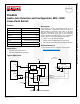
Pin Configuration
M3 = FSA8049UCX Product Identifier
KK = Lot Run Trace Code
X = Year
Y = Work Week
Z = Assembly Site (P= Penang, Malaysia)
● = Pin 1 Indicator
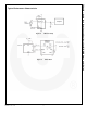
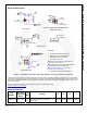
Figure 2. Pin Assignments Figure 3. Top Mark
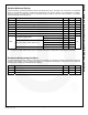
Pin Descriptions
Name Ball Type Description
VDD A1 Power Supply voltage
GNDA A2 GND Switch Ground
(1)
GND/MIC1 A3 I/O Switch connects to audio jack
MIC B1 I/O Switch connects to audio subsystem microphone pre-amplifier
GNDA B2 GND Switch Ground
(1)
GND/MIC2 B3 I/O Switch connects to audio jack
EN C1 Input Enable (0=V
IL
, 1=V
IH
)
0 Disabled
1 Enabled
CEXT C2 Input External capacitor for switch slow t
ON/OFF
timing
GND C3 GND Device Ground
(1)
Note:
1. GND and GNDA can be shorted together if the system does not utilize an FM antenna on the handset ground. If the
system utilizes an FM antenna on the handset ground; separate GND and GNDA, place the FM-decoupling inductor and
capacitor on GNDA only, and connect GND to a low-impedance path to battery ground.
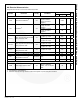
States of Pins after Audio Jack Detection
State of pins GND/MIC1, GND/MIC2, and MIC after detection time (t
DET
) is complete.
GND/MIC1 GND/MIC2 Switch Configuration Accessory Connected
0 (GND) 0 (GND) GND/MIC1=GND, GND/MIC2=GND, MIC=GND 3-Pole Headphones
0 (GND) 1 (MIC Attached) GND/MIC1=GND, GND/MIC2=MIC 4-Pole Headset with Microphone
1 (MIC Attached) 0 (GND) GND/MIC1=MIC, GND/MIC2=GND 4-Pole Headset with Microphone
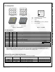
Top Vi ew
Bottom View
13
2
A
B
C
GNDA
VDD
GND
CEXT
EN
GNDA MIC
GND/
MIC1
GND/
MIC2
GNDA
/GND/
MIC1
GNDA
GND/
MIC2
CEXT
GND
A
B
C
123
VDD
EN
MIC
Pin Assignments , Top Through View Pin Assignments Bottom View
Top Mark Side Bump Side
VDD GN DA
GND /
MIC1
MIC GNDA
GND /
MIC2
EN CEXT GND
A
B
C
123
M3 KK
X Y Z