
Datasheet

© 2006 Fairchild Semiconductor Corporation www.fairchildsemi.com
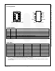
FSA201 Rev. 1.2.2 4
FSA201
USB2.0 Full-Speed and Audio Switches with Negative Signal Capability
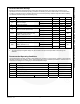
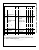
Absolute Maximum Ratings
Stresses exceeding the absolute maximum ratings may damage the device. The device may not function or be
operable above the recommended operating conditions and stressing the parts to these levels is not recommended.
In addition, extended exposure to stresses above the recommended operating conditions may affect device reliability.
The absolute maximum ratings are stress ratings only.
Symbol Parameter Min. Max. Unit
V
AUDIO
/ V
Bus
Supply Voltage -0.5 6.0 V
V
SW
Switch I/O Voltage
(3)
D+, D-, D+/R, D-/L Pins V
BUS
-7.0 V
BUS
+0.3 V
R, L, Pins V
AUDIO
-7.0 V
AUDIO
-0.3 V
A
SEL
Control Input Voltage -0.5 6.0 V
I
IK
Input Clamp Diode Current -50 mA
I
SW
Switch I/O Current (Continuous)
USB 50
mA
Audio 250
I
SWPEAK
Peak Switch Current (Pulsed at 1ms
Duration, <10% Duty Cycle)
USB 100
mA
Audio 500
T
STG
Storage Temperature Range -65 +150 °C
T
J
Maximum Junction Temperature +150 °C
T
L
Lead Temperature (Soldering, 10 seconds) +260 °C
ESD
Human Body Model
(JEDEC: JESD22-A114)
I/O to GND
10
kV
All Other Pins 8
Charged Discharge Model (JEDEC: JESD22-C101) 2
Note:
3. The input and output negative ratings may be exceeded if the input and output diode current ratings are
observed.
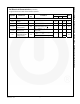
Recommended Operating Conditions
The Recommended Operating Conditions table defines the conditions for actual device operation. Recommended
operating conditions are specified to ensure optimal performance to the datasheet specifications. Fairchild does not
recommend exceeding them or designing to Absolute Maximum Ratings.
Symbol Parameter Minimum Maximum
V
AUDIO
Supply Voltage 2.7V 3.6V
V
BUS
Supply Voltage 4.25V 5.50V
A
SEL
Control Input Voltage 0V V
AUDIO
V
SW
Switch I/O Voltage V
AUDIO
– 6.5V V
AUDIO
– 0.3V
T
A
Operating Temperature -40°C 85°C
JA
Thermal Resistance (free air) MicroPak 10 330ºC / W (estimated)