
Datasheet


FMS6501 — 12 Input / 9 Output Video Switch Matrix with Input Clamp, Input Bias Circuitry, and Output Drivers
© 2004 Fairchild Semiconductor Corporation www.fairchildsemi.com
FMS6501 Rev. 1.0.4 8
I
2
C Interface
Figure 4. Bit Transfer
Figure 5. Definition of START and STOP conditions
Operation
The I
2
C-compatible interface conforms to the I
2
C spec-
ification for Standard Mode. Individual addresses may
be written. There is no read capability. The interface
consists of two lines. These is a serial data line (SDA)
and a serial clock line (SCL), both of which must be
connected to a positive supply through an external
resistor. Data transfer may be initiated only when the
bus is not busy.
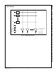
Bit Transfer
One data bit is transferred during each clock pulse.
The data on the SDA line must remain stable during
the HIGH period of the clock pulse. Changes in the line
during this time are interpreted as a control signal.
Data line
stable;
data valid
SCL
SDA
Change
of data
allowed
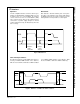
Start and Stop Conditions
The data and clock lines remain HIGH when the bus is
not busy. A HIGH-to-LOW transition of the data line,
while the clock is HIGH, is defined as START condition
(S). A LOW-to-HIGH transition of the data line, while
the clock is HIGH, is defined as STOP condition (P).
SP
START condition
STOP condition
SCL
SDA