
Datasheet


FMS6501 — 12 Input / 9 Output Video Switch Matrix with Input Clamp, Input Bias Circuitry, and Output Drivers
© 2004 Fairchild Semiconductor Corporation www.fairchildsemi.com
FMS6501 Rev. 1.0.4 5
Digital Interface
The I
2
C-compatible interface is used to program output
enables, input to output routing, input clamp / bias, and
output gain. The I
2
C address of the FMS6501 is 0x06
(0000 0110) with the ability to offset it to 0x86 (1000
0110) by tying the ADDR pin high.
Both data and address data, of eight bits each, are writ-
ten to the I
2
C address to access all the control functions.
There are separate internal addresses for each output.
Each output’s address includes bits to select an input
channel, adjust the output gain, and enable or disable
the output amplifier. More than one output can select the
same input channel for one-to-many routing. When the
outputs are disabled, they are placed in a high-imped-
ance state. This allows multiple FMS6501 devices to be
paralleled to create a larger switch matrix. Typical output
power-up time is less than 500ns.
The clamp / bias control bits are written to their own
internal address, since they should always remain the
same regardless of signal routing. They are set based on
the input signal connected to the FMS6501.
All undefined addresses may be written without effect.
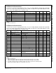
Output Control Register Contents and Defaults
Notes:
1. Power down places the output in a high-impedance state so multiple FMS6501 devices may be paralleled. Power
down also de-selects any input routed to the specified output.
2. When all inputs are OFF, the amplifier input is tied to approximately 150mV and the output goes to approximately
300mV with the 6dB gain setting.
Output Control Register MAP
Notes:
1. IN4 is provided for forward compatibility and should always be written as ‘0’ in the FMS6501.
Clamp Control Register Contents and Defaults
Clamp Control Register Map
Control Name Width Type Default Bit(s) Description
Enable 1 bit Write 0 7 Channel Enable: 1=Enable, 0=Power Down
(1)
Gain 2 bits Write 0 6:5 Channel Gain: 00=6dB, 01=7dB, 10=8dB, 11=9dB
Inx 5 bits Write 0 4:0 Input selected to drive this output: 00000=OFF
(2)
,
00001=IN1, 00010=IN2... 01100=IN12
Register
Name
Register
Address Bit 7 Bit 6 Bit5 Bit4
(1)
Bit3 Bit2 Bit1 Bit0
OUT1 0x01 Enable Gain1 Gain0 IN4 IN3 IN2 IN1 IN0
OUT2 0x02 Enable Gain1 Gain0 IN4 IN3 IN2 IN1 IN0
OUT3 0x03 Enable Gain1 Gain0 IN4 IN3 IN2 IN1 IN0
OUT4 0x04 Enable Gain1 Gain0 IN4 IN3 IN2 IN1 IN0
OUT5 0x05 Enable Gain1 Gain0 IN4 IN3 IN2 IN1 IN0
OUT6 0x06 Enable Gain1 Gain0 IN4 IN3 IN2 IN1 IN0
OUT7 0x07 Enable Gain1 Gain0 IN4 IN3 IN2 IN1 IN0
OUT8 0x08 Enable Gain1 Gain0 IN4 IN3 IN2 IN1 IN0
OUT9 0x09 Enable Gain1 Gain0 IN4 IN3 IN2 IN1 IN0
Control Name Width Type Default Bit(s) Description
Clmp 1 bit Write 0 7:0 Clamp / Bias selection: 1 = Clamp, 0 = Bias
Register Name
Register
Address Bit 7 Bit 6 Bit5Bit4Bit3Bit2Bit1Bit0
CLAMP1 0x1D Clmp8 Clmp7 Clmp6 Clmp5 Clmp4 Clmp3 Clmp2 Clmp1
CLAMP2 0x1E Resv’d Resv’d Resv’d Resv’d Clmp12 Clmp11 Clmp10 Clmp9