
Datasheet


FMS6501 — 12 Input / 9 Output Video Switch Matrix with Input Clamp, Input Bias Circuitry, and Output Drivers
© 2004 Fairchild Semiconductor Corporation www.fairchildsemi.com
FMS6501 Rev. 1.0.4 2
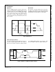
Block Diagram
Figure 1. FMS6501 Block Diagram
C / B
IN1
OUT1 OUT2 OUT9
C / B
IN2
C / B
IN12
SDA
SCL
VCC (2)
GND (2)
Programmable Gain
6, 7, 8, or 9dB
ADDR
Programmable
Enable/Disable