
Datasheet


FMS6501 — 12 Input / 9 Output Video Switch Matrix with Input Clamp, Input Bias Circuitry, and Output Drivers
© 2004 Fairchild Semiconductor Corporation www.fairchildsemi.com
FMS6501 Rev. 1.0.4 12
Layout Considerations
General layout and supply bypassing play major roles in
high-frequency performance and thermal characteristics.
Fairchild offers a demonstration board, FMS6501DEMO,
to use as a guide for layout and to aid in device testing
and characterization. The FMS6501DEMO is a 4-layer
board with a full power and ground plane. For optimum
results, follow the steps below as a basis for high fre-
quency layout.
■ Include 10µF and 0.1µF bypass capacitors.
■ Place the 10µF capacitor within 0.75 inches of the
power pin.
■ Place the 0.1µF capacitor within 0.1 inches of the
power pin.
■ Connect all external ground pins as tightly as possible,
preferably with a large ground plane under the
package.
■ Layout channel connections to reduce mutual trace
inductance.
■ Minimize all trace lengths to reduce series induc-
tances. If routing across a board, place device such
that longer traces are at the inputs rather than the
outputs.
If using multiple, low-impedance, DC-coupled outputs,
special layout techniques may be employed to help dissi-
pate heat.
If a multilayer board is used, a large ground plane
directly under the device helps reduce package case
temperature.
For dual-layer boards, an extended plane can be used.
Worst-case, additional die power due to DC loading can
be estimated at (V
cc
2
/4R
load
) per output channel. This
assumes a constant DC output voltage of V
cc
/2. For 5V
V
cc
with a dual-DC video load, add 25/(4*75) = 83mW,
per channel.
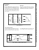
FMS6501 Video Switch Matrix Applications
The increased demand for consumer multimedia sys-
tems has created a challenge for system designers to
provide cost-effective solutions to capitalize on the
growth potential in graphics display technologies. These
applications requires cost-effective video switching and
filtering solutions to deploy high-quality display technolo-
gies rapidly and effectively to the target audience. Areas
of specific interest include HDTV, media centers, and
automotive “infotainment” (includes navigation, in-cabin
entertainment, and back-up camera). In all cases, the
advantages an integrated video switch matrix provides
are high quality video switching specific to the applica-
tion, as well as video input clamps and on-chip, low-
impedance output cable drivers with switchable gain.
Generally the largest application for a video switch is for
the front end of an HDTV, where it takes multiple inputs
and routes them to appropriate signal paths (main pic-
ture and picture in picture - PiP). These are normally
routed into ADCs followed by decoders. There are many
different technologies for HDTV; including LCD, Plasma,
and CRT, with similar analog switching circuitry.
An example of a HDTV application is shown in Figure 14.
This system combines a video switch matrix and two
three-channel switchable anti-aliasing filters. There are
two three-channel signal paths in the system; one for the
main picture, the other for “Picture in Picture” (PiP).
VIPDEMO
TM
Control Software
The FMS6501 is configured via an I
2
C-compatible digital
interface. To facilitate demonstration, Fairchild Semicon-
ductor had developed the VIPDEMO
TM
GUI-based con-
trol software to write to the FMS6501 register map. This
software is included in the FMS6501DEMO kit. Also
included is a parallel port I
2
C adapter and an interface
cable to connect to the demo board. Besides using the
full FMS6501 interface, the VIPDEMO
TM
can also be
used to control single-register read and writes for I
2
C.
Figure 14. HDTV Application using the FMS6501 Video Switch Matrix