
Datasheet


FMS6501 — 12 Input / 9 Output Video Switch Matrix with Input Clamp, Input Bias Circuitry, and Output Drivers
© 2004 Fairchild Semiconductor Corporation www.fairchildsemi.com
FMS6501 Rev. 1.0.4 10
Applications Information
Input Clamp / Bias Circuitry
The FMS6501 accommodates AC- or DC-coupled inputs.
Internal clamping and bias circuitry are provided to sup-
port AC-coupled inputs. These are selectable through
the CLMP bits via the I
2
C compatible interface.
For DC-coupled inputs, the device should be pro-
grammed to use the 'bias' input configuration. In this con-
figuration, the input is internally biased to 625mV through
a 100kΩ resistor. Distortion is optimized with the output
levels set between 250mV above ground and 500mV
below the power supply. These constraints, along with
the desired channel gain, need to be considered when
configuring the input signal levels for input DC coupling.
With AC-coupled inputs, the FMS6501 uses a simple
clamp rather than a full DC-restore circuit. For video sig-
nals with and without sync (Y,CV,R,G,B), the lowest volt-
age at the output pins is clamped to approximately
300mV above ground when the 6dB gain setting is
selected.
If symmetric AC-coupled input signals are used
(chroma,Pb,Pr,Cb,Cr), the bias circuit described above
can be used to center them within the input common
range. The average DC value at the output is approxi-
mately 1.27V with a 6dB gain setting. This value
changes depending upon the selected gain setting.
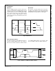
Figure 8 shows the clamp mode input circuit and the
internally controlled voltage at the input pin for AC-cou-
pled inputs.
Figure 8. Clamp Mode Input Circuit
Figure 9 shows the bias mode input circuit and internally
controlled voltage at the input pin for AC-coupled inputs.
Figure 9. Bias Mode Input Circuit
Output Configuration
The FMS6501 outputs may be either AC or DC coupled.
Resistive output loads can be as low as 75Ω, represent-
ing a dual, doubly terminated video load. High imped-
ance, capacitive loads up to 20pF can also be driven
without loss of signal integrity. For standard 75Ω video
loads, a 75Ω matching resistor should be placed in
series to allow for a doubly terminated load. DC-coupled
outputs should be connected as shown in Figure 10.
Figure 10. DC-Coupled Load Connection
If multiple low-impedance loads are DC coupled,
increased power and thermal issues need to be
addressed. In this case, the use of a multilayer board
with a large ground plane to help dissipate heat is rec-
ommended. If a two-layer board is used under these
conditions, an extended ground plane directly under the
device is recommended. This plane should extend at
least 0.5 inches beyond the device. PC board layout
issues are covered in the Layout Considerations section.
AC-coupled loads should be configured as in Figure 11:
Figure 11. AC-Coupled Load Connection
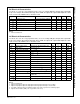
Gain Setting Clamp Voltage Bias Voltage
6dB 300mV 1.27V
7dB 330mV 1.43V
8dB 370mV 1.60V
9dB 420mV 1.80V
FMS6501
Input
Clamp
75
0.1µF
Video source must
be AC-coupled
Lowest voltage
set to 125mV
FMS6501
Input
Bias
75
0.1µF
Video source must
be AC-coupled
Lowest voltage
set to 625mV
75
FMS6501
Output
Amplifier
75
75
FMS6501
Output
Amplifier
220µF
75