
Datasheet


© 2006 Fairchild Semiconductor www.fairchildsemi.com
FMS6346 • Rev. 1.0.5 6
FMS6346 — Six Channel, 6th-Order SD/HD Video FIlter Driver
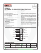
Y
OUT
Driver
Y
IN
0.65V
800kΩ
Applications Information
Functional Description
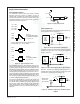
The FMS6346 Low-Cost Video Filter (LCVF) provides
6dB gain from input to output. In addition, the input is
slightly offset to optimize the output driver performance.
The offset is held to the minimum required value to de-
crease the standing DC current into the load. Typical volt-
age levels are shown in Figure 11.
Figure 11. Typical Voltage Levels
The FMS6346 provides an internal diode clamp to sup-
port AC-coupled input signals. If the input signal does not
go below ground, the input clamp does not operate. This
allows DAC out puts to directly drive the FMS6346 without
an AC coupling capacitor. The worst-case sync tip com-
pression due to the clamp does not exceed 7mV. The in-
put level set by the clamp, combined with the internal DC
offset, keeps the output within its acceptable range. When
the input is AC-coupled, the diode clamp sets the sync tip
(or lowest voltage) just below ground.
For symmetric signals like C, U, V, Cb, Cr, Pb, and Pr; the
aver age DC bias is fairly constant and the inputs can be
AC-coupled with the addition of a pull-up resistor to set
the DC input voltage. DAC outputs can also drive these
same signals without the AC coupling capacitor. A con-
ceptual illustration of the input clamp circuit is shown in
Figure 12.
Figure 12. Input Clamp Circuit
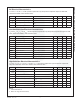
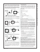
I/O Confi gurations
For DC-coupled DAC drive with DC-coupled outputs, use
the confi guration shown in Figure 13.
Figure 13. DC-Coupled Inputs and Outputs
If the DAC’s average DC output level causes the signal to
exceed the range of 0V to 1.4V, it can be AC-coupled as
shown in Figure 14.
Figure 14. AC-Coupled Inputs, DC-Coupled Outputs
When the is driven by an unknown external source or a
SCART switch with its own clamping circuitry, the inputs
should be AC-coupled as shown in Figure 15.
Figure 15. SCART Confi guration with DC-Coupled
Outputs
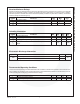
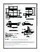
There is a 280mV offset from the DC input level to the
DC output level. V
OUT
= 2 * V
IN
+ 280mV.
0.0 -> 0.02V
0.3 -> 0.32V
0.65 -> 0.67V
1.0 -> 1.02V
V
IN
0.28V
0.88V
1.58V
2.28V
Driven by:
DC-Coupled DAC Outputs
AC-Coupled and Clamped
Y, CV, R, G, B
V
OUT
0.15V
0.5V
0.85V
V
IN
0.58V
1.28V
1.98V
Driven by:
AC-Coupled and Biased
U, V, Pb, Pr, C
V
OUT
DVD or
STB
SoC
DAC
Output
75Ω
LCVF
Clamp
Inactive
0V - 1.4V
DVD or
STB
SoC
DAC
Output
75Ω
LCVF
Clamp
Inactive
0V - 1.4V
DVD or
STB
SoC
DAC
Output
LCVF
Clamp
Active
0.1μF
0V - 1.4V
75Ω
DVD or
STB
SoC
DAC
Output
LCVF
Clamp
Active
0.1μF
0V - 1.4V
75Ω
75Ω
LCVF
Clamp
Active
0.1μF
External video
source must
be AC coupled
0V - 1.4V
75Ω
75Ω
LCVF
Clamp
Active
0.1μF
External video
source must
be AC coupled
0V - 1.4V
75Ω