Hardware Documentation efus™A9X for HW Revision 1.12 and 1.20 and 1.30 efus™A9Xr2 for HW Revision 1.
About This Document This document describes how to use the efus™ start interface board with mechanical and electrical information. The latest version of this document can be found at: http://www.fs-net.de. Important Note! The latest PCB version for efusA9X is Version 1.30, for efusA9Xr2 is Version 1.00. The only difference between these two modules is their Gbit Ethernet PHY’s.
History Date 02.09.15 08.10.15 18.12.15 15.06.16 29.08.16 V 0.1 0.2 0.3 0.4 1.0 Platform All All All All All 06.09.16 1.0 All M M,A R A R A M M A M A A A R A A 19.10.16 03.01.17 19.10.17 1.1 120 220 All All All A A A 26.03.18 230 All 02.08.18 12.12.2018 19.08.2022 17.10.2022 240 240 250 260 All All All All A,M A M A A A V A,M,R Au A,M,R Version Added, Modified, Removed Author Chapter 0 4.9 4.4 7 4.12 4.6 2 4.4 11, 15 3.1 5.2 0 4.7 4 4.13 17, 0 0 10 11 0 3.
Table of Contents About This Document 2 ESD Requirements 2 History 3 Table of Contents 3 1 Block diagram 5 2 Mechanical dimension 6 3 Interface and signal description 7 3.1 4 5 Goldfinger-connector .........................................................................................7 Interfaces 15 4.1 USB host .........................................................................................................15 4.2 USB device ...............................................
10.1 Absolute maximum ratings ..............................................................................30 10.2 DC electrical characteristics for 3.3V IO pins ..................................................30 11 Review service 31 12 ESD and EMI implementing on COM 31 13 Second source rules 31 14 Storage conditions 31 15 ROHS and REACH statement 31 16 Packaging 32 17 Matrix Code Sticker 32 18 Differences efusA9X vs efusA9Xr2 33 19 Appendix 34 Important Notice ...........
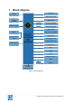
1 Block diagram 5V Power In DDR3 USB 2.0 Device/Host SLC NAND Flash up to 1GB or Quad SPI USB 2.0 Host eMMC up to 32GB LAN Phy LAN (10/100/1000Mb) LAN Phy LAN (10/100/1000Mb) RGB LCD 18bit Ext. RTC High Accuracy RTC (TXCO) JTAG Connector Single Channel LVDS 24bit Freescale i.MX 6SoloX Cortex-A9/-M4 CPU up to 1GHz/200MHz Digital Camera Analog Camera (1-4) 4x UART (2x RTS/CTS) 2x CAN 2.
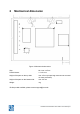
2 Mechanical dimension Figure 2: Mechanical dimensions Size: 62.11mm x 47mm PCB thickness: 1.2 ± 0.1mm Height of the parts on the top side: max. 4.5 mm (except Jtag connector not mounted on mass production) Height of the parts on the bottom side: max. 2.0 mm Weight: 14g 3D Step model available, please contact support@fs-net.
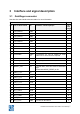
3 Interface and signal description 3.1 Goldfinger-connector See also efus start interface documentation for more information. J1 Pin Use on base board I/O Remarks; onboard pullups 1.12-> 1.20 change 1 +5V Power In PWR 2 +5V Power In PWR 3 +5V Power In PWR 4 +5V Power In PWR 5 +5V Power In PWR 6 +5V Power In PWR 7 GND PWR 8 GND PWR 9 VBAT In PWR RTC battery input 10 V33-Enable PWR/ O5 3.3V/100mA out, use as enable for main board 3.
J1 Pin Use on base board I/O 27 GND PWR 28 SD_A_CLK O5*# 29 CAN_A_TX O5* 30 GND PWR 31 CAN_A_RX I* 32 SD_A_DAT0 I/O*# 33 GND PWR 34 SD_A_DAT1 I/O *# 35 CAN_B_TX O5* 36 NC 37 CAN_B_RX 38 NC 39 GND 40 NC 41 MPCIE_CTX_P 42 NC 43 MPCIE_CTX_N 44 NC 45 GND PWR 46 GND PWR 47 MPCIE_CRX_P Idiff # 48 EXT_PROG 49 MPCIE_CRX_N Idiff # 50 SPI_B_MISO I* 51 GND PWR 52 SPI_B_MOSI O5* 53 MPCIE_CLK_P Odiff # 54 SPI_B_SPCK O5* 55 MPCIE_CLK_N Odiff #
J1 Pin Use on base board I/O Remarks; onboard pullups 60 SPI_B_IRQ1 I* 100k pull-up 61 MPCIE_WAKE I 62 SPI_B_IRQ2 I* 63 GND PWR 64 GND PWR 65 SD_B_DAT2 I/O* 66 SPI_A_MISO I* 67 SD_B_DAT3 I/O * 68 SPI_A_MOSI O5* 69 SD_B_CMD O5* 70 SPI_A_SPCK O5* 71 SD_B_VCC PWR 72 SPI_A_CS1 O5* 73 SD_B_CLK O5* 74 SPI_A_CS2 O5* 75 GND PWR 76 SPI_A_IRQ1 I* 100k pull-up 77 SD_B_DAT0 I/O* 100k pull-up 78 SPI_A_IRQ2 I* 100k pull-up 79 SD_B_DAT1 I/O* 80 GND PWR
J1 Pin Use on base board I/O 93 LCD_CLK O5* 94 TXD_A_TTL O5* 95 GND PWR 96 RXD_D_TTL I* 97 LCD_HSYNC O5* 98 TXD_D_TTL O5* 99 LCD_VSYNC O5* 100 GND PWR 101 GND PWR 102 RXD_B_TTL I* 103 LCD_R0 O5* 104 TXD_B_TTL O5* 105 LCD_R1 O5* 106 RTS_B_TTL O5* 107 LCD_R2 O5* 108 CTS_B_TTL I* 109 LCD_R3 O5* 110 GND PWR 111 LCD_R4 O5* 112 I2S_MCLK O5* 113 LCD_R5 O5* 114 GND PWR 115 GND PWR 116 I2S_LRCLK O5* 117 LCD_G0 O5* 118 GND PWR 119 LCD_G1 O5* 120 I2S_SCLK
J1 Pin Use on base board I/O 126 I2S_DIN O5* 127 LCD_G5 O5* 128 GND PWR 129 GND PWR 130 I2C_C_DAT I/O 131 LCD_B0 O5* 132 I2C_C_CLK I/O 133 LCD_B1 O5* 134 DVI_DDC_VOUT PWR 135 LCD_B2 O5* 136 GND PWR 137 LCD_B3 O5* 138 NC 139 LCD_B4 I/O* I* X LVDS_TX1_DP available on a special version with minimum order quantity X LVDS_TX1_DN available on a special version with minimum order quantity X LVDS_TX0_DP available on a special version with minimum order quantity X LVDS_TX0_DN avai
J1 Pin Use on base board I/O 1.12-> 1.
J1 Pin Use on base board I/O Remarks; onboard pullups 189 CAM_VCAM PWR Camera interface voltage out (default 2.8V) Other voltages on request 190 ETH_A_D4_P I/Odiff 191 CAM_HREF I/O(*) parallel camera signal 192 ETH_A_LED_ACT O5 LINK/ACT (on with link, blinking with activity) 193 CAM_PWDN 1.12-> 1.
J1 Pin Use on base board I/O Remarks; onboard pullups 1.12-> 1.20 change 220 NC 221 USB_DEV_OC I* 222 NC 223 USB_DEV_ID I 224 GND PWR 225 USB_DEV_N I/Odiff 100k pull up 226 NC 227 USB_DEV_P I/Odiff 228 NC 229 GND PWR 230 GND PWR Table 1: 230 pin goldfinger connector O5: 3.3V 5mA logic output I: 3.3V logic input Idiff, Odiff, I/Odiff: differential signal PWR: Power input or output *: SW configurable as GPIO; 3.3V logic level (*): 2.
4 Interfaces 4.1 USB host The 90 Ohm differential pair of USB signals doesn't need any termination. For external ports ESD and EMV protection is required nearby the USB connector. 212 USB_A_PWRON High active USB port power on signal 214 USB_A_N Differential USB Signal 216 USB_A_P 4.2 USB device The 90 Ohm differential pair of USB signals don't need any termination. For external ports ESD and EMV protection is required nearby the USB connector. 217 USB_DEV_VBUS 4.6 … 5.
4.4 SD/MMC card The interface is supporting a SD card channel. For specification and licensing please refer the website of the SD Association http://www.sdcard.org. Unused signals should be left unconnected. No.
4.5 SPI The module support 2 HS SPI (Serial Peripheral Interface) with 2 chip selects and 2 interrupt inputs. All signals are 3.3V compliant and do have pull-up on module. Devices on baseboard with other voltage need a level shifter.
4.6 I2C The module supports a I2C interface as I2C master. Signals are 3.3V compliant and do have pull-up on module. Devices on baseboard with other voltage need a level shifter. 82 I2C_B_DAT Data signal 4k7 PU onboard 84 I2C_B_CLK Clock signal 4k7 PU onboard 86 I2C_B_IRQ Optional interrupt input 100k PU onboard 88 I2C_B_RST Optional reset output 100k PU onboard A second I2C output is reserved for display control and a touch controller for resistive or capacitive touch.
4.
4.9 Ethernet The module supports 2 10/100/1000 Mbit LAN interfaces. The only difference between these two modules is their Gbit Ethernet PHY’s. efus™A9X Qualcomm Atheros AR8035 efus™A9Xr2 Realtek RTL8211F/D 186 ETH_CTREF Common power pin for both LAN transformer 188 ETH_A_D4_N Differential data line 190 ETH_A_D4_P 192 ETH_A_LED_ACT LINK/ACT (on with link, blinking with activity), serial R needed 194 ETH_A_D3_N Differential data line 196 ETH_A_D3_P 198 ETH_A_VLEDOUT 3.
4.10 PCIe A single lane PCI Express port (Gen 2.0) is supported. Please following design rules from PCI-SIG on your design.
4.11 RGB LCD 87 BL_CTRL 3.3V CMOS PWM output for Backlight dimming 89 VCFL_ON CMOS 3.
4.12 Parallel Camera (CSI) Note: because an HW failure this pinout is just working HW Revision ≥1.20! 161 n.a./ CAM_YDATA0 I (2.8V) * CPU pad QSPI1A_SS0 163 n.a./ CAM_YDATA1 I (2.8V) * CPU pad QSPI1A_SCLK 165 CAM_YDATA4 I (2.8V) CPU pad CSI_DATA02 167 CAM_YDATA3 I (2.8V) CPU pad CSI_DATA01 169 CAM_YDATA5 I (2.8V) CPU pad CSI_DATA03 171 CAM_YDATA2 I (2.8V) CPU pad CSI_DATA00 173 CAM_YDATA6 I (2.8V) CPU pad CSI_DATA04 175 CAM_PCLK I (2.
4.14 MISC 10 V33-Enable 3.3V/100mA Vout, use as enable for main board 3.3V regulator if more current is required 11 ACOK USB OTG charge detect, future use 12 !RESET_IN 3.3V 100k pull-up on module drives with OC/OD to GND. Leave open if not used. 14 !RESET_OUT 4.7k pull down, active low reset for baseboard logic 25 PWM_A 3.3V TTL level PWM output 5 Flash 5.1 NAND Flash By default, boot mode of efusA9 is configured for NAND boot.
5.4 I2C EEPROM This component is optional and not mounted in all configurations. Please contact sales to get more information. 6 Power +5V Power In VCC in, 5V +/-5% GND GND, connect all GND pins to GND plane VBAT In RTC battery input. Leave open if not used V33-Enable 3.3V/max. 100mA Vout use as enable for main board 3.3V regulator if more current is required VLCD (on LVDS connector) 3.3V/max.
7 LVDS-connector The LVDS display port can be direct connected to a LVDS 18 or 24 bit single channel. Display is independent from RGB LCD. JILI30 JAE FI-X30SSLA Connector or compatible GF pin option Pin Function 28..30 VLCD (3.3V or 5V software configurable, max.
7.1 LVDS EMI filtering The following schematic shows the internal connection of LVDS signals between connector and CPU. The common mode chokes are TDK MCZ2010CH240L4T, Panasonic EXC28CG240U or equivalent parts.
8 WLAN/ BT Starting HW Revision 1.20 efusA9X can provide a 802.11b/g/n/ac and BT4.1 + HS “Smart Ready” BLE solution based on QCA9377 chipset with U.FL connector for an external antenna on module. The “Letter of Conformity” for this RF functionality excluding 802.11ac is available from our homepage. Our pre-approval is just re-usable by using the antennas listed on this letter. In a customized version with minimum order quantity a GHz chip antenna for an external antenna can be mounted instead the U.
P/N: AH104N2450D1 Peak gain: 2.1 dBi (2.4GHz), 2.4 dBi (5GHz) RF exposure considerations Consistent with §2.909(a), the following text must be included within the user’s manual or operator instruction guide for the final commercial product: This modular complies with FCC RF radiation exposure limits set forth for an uncontrolled environment. This transmitter must not be co-located or operating in conjunction with any other antenna or transmitter.
10 Electrical characteristic VCC: 5V +/- 5% VBAT In for RTC: 2.2 … 3.45V power consumption typical current consumption BATT: 3 µA maximum power consumption BATT: 10 µA @25°C Thermal design power (summary all chips) With 1GHz SoloX CPU 5.5 Watt @25°C Additional with Wifi mounted +1.
11 Review service F&S provide a schematic review service for your baseboard implementation. Please send your schematic as searchable PDF to support@fs-net.de. 12 ESD and EMI implementing on COM Like all other COM modules at the market there is no ESD protection on any signal out from the COM module. ESD protection hast to place as near as possible to the ESD source - this is the connector with external access on the COM baseboard. A helpful guide is available from TI; just search for slva680 at ti.com.
16 Packaging All F&S ESD-sensitive products are shipped either in trays or bags. efus™ modules are shipped in trays. One tray can hold 10 boards. An empty tray is used as top cover. Figure 3: Tray for shipment 17 Matrix Code Sticker All F&S hardware is shipped with a matrix code sticker including the serial number. Enter your serial number here https://www.fs-net.de/en/support/serial-number-info-and-rma/ to get information on shipping date and type of board.
18 Differences efusA9X vs efusA9Xr2 The difference between efusA9X and efusA9Xr2 is the Ethernet Phy. efusA9X Qualcomm AR8035-AL1 efusA9Xr2 Realtek RTL8211FD Both Phys are Gbit Phys and are connected by RGMII interface to CPU. All frequencies are the same. In the below picture we marked the area with changes.
19 Appendix Important Notice The information in this publication has been carefully checked and is believed to be entirely accurate at the time of publication. F&S Elektronik Systeme assumes no responsibility, however, for possible errors or omissions, or for any consequences resulting from the use of the information contained in this documentation.
Disclaimer of Warranty THIS WARRANTY IS MADE IN PLACE OF ANY OTHER WARRANTY, WHETHER EXPRESSED, OR IMPLIED, OF MERCHANTABILITY, FITNESS FOR A SPECIFIC PURPOSE, NON-INFRINGEMENT OR THEIR EQUIVALENTS UNDER THE LAWS OF ANY JURISDICTION, EXCEPT THE WARRANTY EXPRESSLY STATED HEREIN. THE REMEDIES SET FORTH HEREIN SHALL BE THE SOLE AND EXCLUSIVE REMEDIES OF ANY PURCHASER WITH RESPECT TO ANY DEFECTIVE PRODUCT.