
Specifications

78 SAM0025A-062397 ESS Technology, Inc.
ES1879 DATA SHEET
REGISTERS
PRELIMINARY
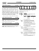
Test Register (7Eh, R/W)
This register is a test register.
Bits Definitions:
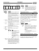
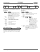
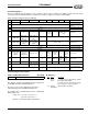
Table 26 Test Bus Assignments
ADC test
enable
Test bus
enable
MIDI loop-
back test
FM test
enable
DSP loop-
back test
2nd DMA
test enable
0
7654 3 2 1 0
Bits Name Description
7 ADC test
enable
1 = ADC logic test mode:
GPI replaces left ADC comparator input and
Spatializer ADC comparator input; inverted
GPI replaces right ADC comparator input.
6:5 Test bus
enable
When either of these bits is high, signals
between the digital and analog parts of the
chip are available via an e-bit output bus con-
sisting of:
TST[7:0] = {DRQB, IRQE, IRQD, IRQC, IRQB,
GPO2, GPO1, GPO0}
The data on the bus is selected by a 4-bit
select code:
SEL[3:0] = {SWD, SWC, SWB, SWA}
See Table 26 below.
4MIDI
loopback
test
1 = MSO is internally connected to MSI, loop-
ing back the MIDI transmitted from either the
MPU-401 port or the Sound Blaster-compatible
method.
0 = Disable MIDI loopback test.
3FM test
enable
1 = The four normal FM registers can only be
accessed via Audio_Base+0h to
Audio_Base+3h. Four FM test registers are
accessed via 388h to 38Bh.
2 DSP
loopback
test
1 = DSP loopback test mode enabled.
1. Internally, data that would normally be
transmitted out DX is looped back to
replace data normally received by DR.
2. The ES689/69x serial interface data
has a 32-bit shift register. The shift out
data from the last stage appears on the
DX pin.
3. The 125 Hz clock used by hardware
volume control and the DRQ latch
circuits is sped up by a factor of four.
0 = DSP loopback test mode disabled.
12nd
DMA test
enable
1 = Enable second DMA test mode. Reading
mixer register 74h returns data from the audio
2 FIFO and acts as a sample rate strobe to the
FIFO in place of the normal sample rate gener-
ator.
0 = Disable second DMA test mode.
0 – Reserved. Always write zero.
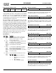
SEL[3:0]
TST[7:0] in Test Mode 1
TST[7:0] in Test Mode 2
0
DAC/ADC1 data left [7:0]
DAC2 data left [7:0]
1
DAC/ADC1 data left [15:8]
DAC2 data left [15:8]
2
DAC/ADC1 data right [7:0]
DAC2 data right [7:0]
3
DAC/ADC1 data right [15:8]
DAC2 data right [15:8]
4
Music DAC data left [7:0]
Spatializer ADC data [7:0]
5
Music DAC data left [15:8]
Spatializer ADC data [15:8]
6
Music DAC data right [7:0]
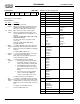
7:4 XSEL[3:0]
3:2 XMIX[1:0]
1 IETPG
0 IHOLD
7
Music DAC data right [15:8]
SPGAIN [7:0]
8
7 MOEN
6 EN26DB
5:4 SRCSEL[1:0]
3 PDN
2 CCK
1 FILTCLK2
0 FILTCLK1
7 ENSPZR
6 SPCLK
5 SPMONO
4 SPEVIN
3 –
2 SPETPG
1 SPADCLK
0 SPLR
9
7 CAL
6:5 MOSEL[1:0]
4 ADCMODE1
3 ADCMODE0
2 MONOE
1 SCFBYP2
0 SCFBYP1
FBC[7:0]
10
7 ADCLK
6 EVIN1R
5 HOLD1R
4 ETPG1R
3 EVIN1L
2 HOLD1L
1 ETPG1L
0 MISEL
FBC[15:8]
11
7:6 FSELR[1:0]
5:4 FSELL[1:0]
3 HOLD2
2 ETPG2
1 FMHOLD
0 FMETPG
FBC[23:16]
12
7:4 IVOLR[3:0]
3:0 IVOLL[3:0]
I
2
S data left[7:0]
13
7 OVOLR[8]
6 OVOLL[8]
5:4 MIXSEL[1:0]
3:2 OSELR[1:0]
1:0 OSELL[1:0]
I
2
S data left[15:8]
14
OVOLL[7:0]
I
2
S data right[7:0]
15
OVOLR[7:0]
I
2
S data right[15:8]