
Specifications

6 SAM0025A-062397 ESS Technology, Inc.
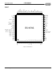
ES1879 DATA SHEET
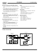
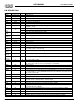
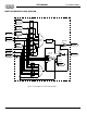
PIN DESCRIPTION
PRELIMINARY
PIN DESCRIPTION
Name Number I/O Description
GNDD 1, 24, 61, 78 I Digital ground.
A[11:0] 13:2 I ISA address bus.
AEN 14 I ISA address valid when active-low, DMA when high.
VDDD 15, 74, 100 I Digital power supply (3.0 - 5.5 V).
D[7:0] 23:16 I/O ISA data bus. 24 mA drivers.
SW(A-D) 28:25 I Joystick switch inputs. These pins have internal pull-ups to VDDD.
T(A-D) 32:29 I/O Joystick timers. Use the digital power supply. These pins have internally weak pull-downs
to GNDD (> 1M Ω).
AUXB_L
33
I Aux B input, left. 50k Ω pull-up to CMR.
FDXI I Used with DSP interface as line-level mono input (25k Ω input impedance).
AUXB_R
34
I Aux B input, right. 50k Ω pull-up to CMR.
FDXO O Used with DSP interface as line-level mono output, capable of driving a 5k Ω load.
AUXA_L,
AUXA_R
35,36 I Aux A (CD) inputs, left and right. 50k Ω pull-ups to CMR.
CMR 37 O 2.25 V reference buffer output.
MIC 38 I Mic input to +26 dB internal preamp. 80k Ω pull-up to CMR.
GNDA 39, 55 I Analog ground.
CAP3D 40 O Bypass capacitor to GNDA for 3-D effect.
VDDA 41 I Analog power supply, 4.75 - 5.25 V.
FOUT_L,
FOUT_R
43:42 O Filter outputs, left and right. These pins are normally AC coupled to CIN_L and CIN_R.
The output resistance is about 5k Ω.
CIN_L,
CIN_R
44, 45 I Capacitive coupled inputs, left and right. The input resistance is about 50k Ω.
LINE_L,
LINE_R
46, 47 I Line inputs, left and right. 50k Ω pull-ups to CMR.
AOUT_L,
AOUT_R
48, 49 O Analog outputs, left and right, from master volume. These pins can drive a 5k Ω load.
PCSPKO 50 O PC speaker analog output.
XA[3:0] 51, 52, 53, 54 I/O Bidirectional differential transmitter/receivers. Expansion audio bus. These are analog sig-
nals that are DC-coupled to the corresponding pins of the ES978.
GNDA 55 I Analog ground.
XSD 56 I/O Expansion serial bus data I/O. High-impedance when DOCKED = 0.
XSC 57 O/Hi Z Expansion serial bus clock and frame sync. High-impedance when DOCKED = 0.
IPROM 58 I Select between internal PnP ROM and external EEPROM for Plug and Play configuration.
1 = internal ROM, 0 = external EEPROM. ES1878 function PNPEN is replaced by bit 2 of
PnP Vendor register 2Dh.
MSO 59 O MIDI serial output.
MSI 60 I MIDI serial input. MSI has an internal pull-up to VDDD.
DX 62 O/Hi Z Serial data transmit. Active output when data is being transmitted serially from the
ES1879; otherwise, high impedance. Tri-state output.
DR 63 I Serial data receive. This pin has an internal pull-down to GNDD.
DCLK 64 I Serial clock input. This pin has an internal pull-down to GNDD.
FS 65 I Frame sync input. Software-programmable to be active-high or active-low. This pin has
an internal pull-down to GNDD.
MCLK 66 I Serial clock input from ES689/ES69x. This pin has an internal pull-down to GNDD.
MSD 67 I Serial data input from ES689/ES69x. This pin has an internal pull-down to GNDD.
IIDATA 68 I
Serial data for I
2
S interface. This pin has an internal pull-down to GNDD.
IISCLK 69 I
Serial shift clock for I
2
S interface. This pin has an internal pull-down to GNDD. I
2
S
IILR 70 I
Left/right signal for I
2
S interface. This pin has an internal pull-down to GNDD.