
Specifications

ESS Technology, Inc. SAM0025A-062397 45
ES1879 DATA SHEET
I/O PORTS
PRELIMINARY
FM Device
The FM synthesizer operates in two different modes:
Emulation mode and Native mode. In Emulation mode, the
FM synthesizer is fully compatible with the OPL3 FM
synthesizer. In Native mode, the FM synthesizer has
increased capabilities and performance for more realistic
music. The following register descriptions are for
Emulation mode only.
FM Status (FM_Base+0h, R)
Reading this register returns the overflow flags for timers
1 and 2 and the “interrupt request” from these timers (this
is not a real interrupt request but is supported as a status
flag for backward compatibility with the OPL3 FM
synthesizer).
FM Low Bank Address (FM_Base+0h, W)
Low bank register address.
NOTE:
Any write to this register will also put the FM
synthesizer in Emulation mode if it is currently in Native
mode.
FM Data Write (FM_Base+1h, W)
FM register write. The data written to FM_Base+1h is
written to the current address FM register. Note that
register writes must follow the timing requirements of the
OPL3 FM synthesizer.
FM High Bank Address (FM_Base+2h, W)
High bank register address.
FM Data Write (FM_Base+3h, W)
FM register write. Writing to this register in Emulation
mode is the same as writing to register FM_Base+1h.
MPU-401 Device
MPU-401 Data (MPU_Base+0h, R/W)
This register is used to read data from the MPU-401
receive FIFO or a command acknowledge byte (0FEh).
This register is also used to write data to the MPU-401
transmit FIFO.
MPU-401 Command (MPU_Base+1h, W)
The MPU-401 device accepts only two commands:
FFh Reset/return to Smart mode. This command
generates an acknowledge byte if received
when already in Smart mode.
3Fh Go to UART mode. This command generates
an acknowledge byte if received while in
Smart mode. It is ignored if the device is
already in UART mode.
MPU-401 Status (MPU_Base+1h, R)
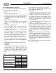
Bit Definitions:
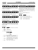
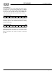
IRQ FT1 FT2 0 0 0 0 0
76543210
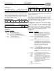
A7 A6 A5 A4 A3 A2 A1 A0
76543210
D7 D6 D5 D4 D3 D2 D1 D0
76543210
A7 A6 A5 A4 A3 A2 A1 A0
76543210
D7 D6 D5 D4 D3 D2 D1 D0
76543210
D7 D6 D5 D4 D3 D2 D1 D0
76543210
D7 D6 D5 D4 D3 D2 D1 D0
76543210
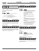
-RR -TR x
76543210
Bits Name Description
7 -RR 0 = read data available in the receive FIFO, or
pending acknowledge byte to be read
(0FEh).
6 -TR 0 = there is room in the transmit FIFO to accept
another byte.
5:0 – Don’t care.