
Specifications

ESS Technology, Inc. SAM0025A-062397 33
ES1879 DATA SHEET
CONFIGURATION
PRELIMINARY
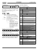
Vendor-Defined Card-Level Registers (20h – 2Fh)
This section describes the PnP Vendor registers of the
ES1879.
IRQB, IRQA (20h, R)
Defines IRQ number assigned to B and A pins. Loaded
from configuration ROM header after PnP reset. Unused
IRQ pins should be assigned IRQ #1.
IRQD, IRQC (21h, R)
Defines IRQ number assigned to D and C pins. Loaded
from configuration ROM header after PnP reset. Unused
IRQ pins should be assigned IRQ1.
IRQE (22h, R)
Bits 3:0 define IRQ number assigned to E pin. Loaded from
configuration ROM header after PnP reset. If the IRQ pin is
unused, it should be assigned IRQ1. Bits 7:4 are reserved.
Always write 0.
DRQB, DRQA (23h, R)
Defines DRQ number assigned to B and A pins. Loaded
from configuration ROM header after PnP reset. Unused
DRQ pins should be assigned DRQ2.
DRQD, DRQC (24h, R)
Bits 3:0 define DRQ number assigned to C pins. Bits 7:4
define DRQ number assigned to D pins. If DRQD and
DACKBD are not connected to an ISA DMA channel, then
these pins should be assigned DRQ2. Loaded from
Configuration ROM header after PnP reset.
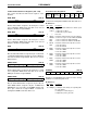
Shared Function Assignment (25h, R)
Loaded from Configuration ROM header after PnP reset.
Bit Definitions:
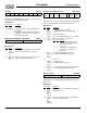
GPO Map (26h, R)
One bit for each GPO[6:0]. This register is reset to zero by
hardware reset, but not by PnP reset.
Bit Definitions:
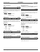
IRQB IRQA
76543210
IRQD IRQC
76543210
0IRQE
76543210
DRQB DRQA
76543210
DRQD DRQC
76543210
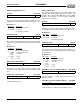
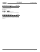
MPU-401
LDN 1/
LDN 3
x
VOLUP,
VOLDN/
GPI5, GPI6
MUTE/
GPI4
IRQE/
GPO6
IRQD/
GPO5
IRQC/
GPO4
IRQB/
GPO3
76 5 4 3 2 1 0
Bits Name Description
7 MPU-
401 LDN
1/LDN 3
Determines whether MPU-401 is LDN 3 or part
of LDN 1.
1 = MPU-401 is LDN 3.
0 = MPU-401 is part of LDN 1.
6 — Don’t care.
5VOLUP,
VOLDN/
GPI5,
GPI6
Determines which functions pins 91 and 92 are
used for. These pins are also SEDI and SEDO.
1 = Pins 91 and 92 are GPI5 and GPI6.
0 = Pins 91 and 92 are VOLUP and VOLDN.
4MUTE/
GPI4
Determines which function pin 90 is used for.
1 = Pin 90 is GPI4.
0 = Pin 90 is MUTE.
3IRQE/
GPO6
Determines which function pin 93 is used for.
1 = Pin 93 is GPO6.
0 = Pin 93 is IRQE.
2IRQD/
GPO5
Determines which function pin 94 is used for.
1 = Pin 94 is GPO5.
0 = Pin 94 is IRQD.
1IRQC/
GPO4
Determines which function pin 95 is used for.
1 = Pin 95 is GPO4.
0 = Pin 95 is IRQC.
0IRQB/
GPO3
Determines which function pin 96 is used for.
1 = Pin 96 is GPO3.
0 = Pin 96 is IRQB.
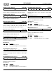
x GPO6 GPO5 GPO4 GPO3 GPO2 GPO1 GPO0
76543210
Bits Name Description
7 — Don’t care.
6:0 GPO[6:0] 1 = GPO pin controlled by corresponding GPI
pin of the ES978.
0 = GPO pins controlled by port
Configuration_Device_Base+2h.