
Specifications

30 SAM0025A-062397 ESS Technology, Inc.
ES1879 DATA SHEET
CONFIGURATION
PRELIMINARY
Accessin
g
the ROM/EEPROM
The PnP ROM/EEPROM software interface is used to
directly read the PnP ROM or EEPROM, as well as send
commands and data to program an external EEPROM.
See “Serial EEPROM Interface” on page 27.
PnP Confi
g
uration and Re
g
isters
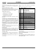
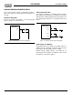
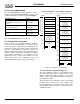
Figure 16 shows the configuration register set that is
discussed in the following pages. As shown below, the
Card-Level registers supported by the ES1879 are the
Card-Control Card-Level registers at addresses 00h-07h,
and the Vendor-Defined Card-Level registers at
addresses 20h-2Fh. The Card-Control Card-Level register
at address 07h is a pointer to the Logical Device registers
supported by the ES1879 (one set of registers for each
logical device on the “card”). In the ES1879, there are
three logical devices: the configuration device, the
audio+FM+MPU-401 device, and the joystick device.
Figure 16 Configuration Register Outline
Accessing the PnP Configuration Registers
The PnP configuration registers of the ES1879 can be
accessed in two ways. First, the registers can be read or
written as defined by the PnP specification. Second, the
registers can be read or written using two I/O locations of
the configuration device.
The first location of the configuration device is written with
the PnP register number to be read or written. After
programming the PnP register number, the register can be
read or written by accessing the second location of the
configuration device.
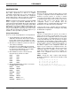
EEPROM Function Action
Read EEPROM data register or read
internal ROM, then increment one
address.
Read PnP Vendor
register 2Eh.
Write EEPROM data register, then
increment one address.
Write PnP Vendor
register 2Eh.
Write EEPROM command register. Write PnP vendor
register 2Fh.
Reset EEPROM/ROM address
counter.
Read PnP vendor
register 2Fh.
Address
00h
01h
02h
03h
04h
05h
06h
07h
Address
30h
31h
32h
37h
Set Read Port Address
Serial Isolation
Configuration Control
Wake Command
Resource Data
Status
Card Select Number (CSN)
Logical Device Number
Reserved
Card-Level
Registers
Vendor-Defined
Card-Level
Registers
Vendor-Defined
Logical Device
Control
Activate
I/O Range Check
Reserved for
Logical Device
Control
ISA Memory
Configuration
Registers 3:0
I/O Configuration
Registers 7:0
Interrupt Configuration
Registers 1:0
DMA Configuration
Registers 1:0
32-bit Memory
Configuration
Reserved for
Logical Device
Configuration
Vendor-Defined
Logical Device
Configuration
Reserved
Registers 1:0
38h
3Fh
70h
73h
60h
6Fh
•
•
•
40h
5Fh
A9h
EFh
F0h
FEh
76h
A8h
74h
75h
FFh
08h
1Fh
20h
2Fh
Card-Level Registers
(one set per card)
Logical Device Registers
(one set per logical device on card)
•
•
•
•
•
•
•
•
•
•
•
•
•
•
•
•
•
•
•
•
•
•
•
•
•
•
•
•
•
•
(Not supported)
(Not supported)
(Not supported)
(Not supported)
(Not supported)
(Not supported)
(Not supported)
8 bits
70
8 bits
70
Card-Control Card-Level Registers