
Specifications

ESS Technology, Inc. SAM0025A-062397 29
ES1879 DATA SHEET
CONFIGURATION
PRELIMINARY
CONFIGURATION
The ES1879 supports the industry-standard ISA Plug and
Play (PnP) specification, as well as a software
configuration method that does not rely on PnP. Bit 2 of
PnP vendor register 2Dh determines the configuration
method. When bit 2 is high, the ISA PnP configuration
mode is disabled. Bit 2 is low (ISA PnP) by default.
NOTE:
The ES1878 supported PnP from an internal ROM
and/or a bypass key. External EEPROM was not
supported. An input pin PNPEN, when high, enabled both
PnP and a bypass key written to I/O address 279h. When
PNPEN was low, PnP was disabled and the bypass key
was written to I/O address 388h. In the ES1879, the
function of pin PNPEN is replaced by bit 2 of PnP vendor
register 2Dh. The ES1879 also allows the bypass key to
be written to either port 279h or port 388h.
Usin
g
ISA PnP Mode
There are several design implications of using ISA PnP:
1. The PCI-ISA bridge for the ES1879 must be in
subtractive decode mode. This mode is required
because PnP can place the I/O addresses of the
ES1879 devices in a very large number of locations.
2. All PnP devices within the system must share the
same ISA bus and bridge.
3. The internal resource ROM cannot be changed.
I/O addresses, interrupts, and DMA channels must
be supported as defined by the resource ROM.
The joystick port must be supported.
4. All five IRQ lines must be connected to ISA
interrupt request channels as follows:
IRQA -IRQ9
IRQB -IRQ5
IRQC -IRQ7
IRQD -IRQ10
IRQE -IRQ11
5. All three DRQ/DACK pairs must be connected to
ISA DMA signals as follows:
DRQA DRQ0
DACKBA -DACK0
DRQB DRQ1
DACKBB -DACK1
DRQC DRQ3
DACKBC -DACK3
DRQD DRQ5, 6, or 7
DACKBD -DACK5, 6, or 7
Non PnP Mode
Because of the above restrictions imposed by use of PnP,
a separate configuration method is implemented in the
ES1879. A special sequence of 34 bytes is written
consecutively to I/O address 279h or 388h. This sequence
is called the “bypass key” because it can be used to short-
circuit the PnP process and directly enable the
configuration device of the ES1879. Once the
configuration device is enabled, all the PnP registers of the
ES1879 are accessible and can be programmed.
Using Non PnP mode is advisable when the ES1879 is
designed into the motherboard. Send bypass key during
the BIOS PnP configuration.
Bypass Key
If PnP is not supported by the system, it is possible to
bypass PnP by issuing a special “bypass key” to the
ES1879 to force the configuration device to be enabled at
a specific l/O address. The ES1879 must be in the “wait-
for-key” Plug and Play state. The special key is 32 bytes
long, written to the PnP address register (279h or 388h).
Follow the bypass key immediately with two I/O writes to
the PnP address register to set the low and high bytes of
the address register of the configuration device. The
bypass key also activates the configuration device. The
address of the configuration device must be in the range
100h-FF8h, aligned on a multiple of 8. An “alias” of the
audio device address can be used. For example, use
E20h for the configuration device if the audio device
address is at 220h.
NOTE:
Perform the entire sequence with interrupts
disabled to minimize the chance that an interrupt corrupt
the sequence.
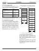
66, a1, c2, f1, ea, e7, 71, aa
c7, 63, 33, 1b, d, 96, db, 6d
a4, 50, 28, 16, 9b, 4d, b6, c9
f4, 78, 3e, 8d, d6, fb, 7f, 3d
<config_address_low>, <config_address_high>