
Specifications

ESS Technology, Inc. SAM0025A-062397 25
ES1879 DATA SHEET
PERIPHERAL INTERFACING
PRELIMINARY
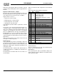
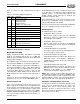
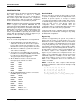
Table 11 contains the data configuration for the upload
period.
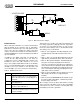
Expansion Audio Interface – Analog
Mono FDXI and FDXO
FDXI is shared with AUXB_L and FDXO is shared with
AUXB_R. The ES1879 supports the use of FDXI and
FDXO as input to the ADC and output from the DAC when
using the DSP serial port.
Mono FDXI/O mode is useful with an external modem that
has integrated a CODEC for speakerphone applications.
Bits 1:0 of Mixer Extension register 46h enable FDXI as a
mono input and FDXO as a mono output. When FDXI is a
mono input to the mixer, its input impedance is cut in half
to 25k ohms. When FDXO is an output, it has a 5k ohm
output impedance. When FDXO is not an output, it is the
AUXB_R input to the mixer and has a 50k ohm pull-up to
CMR.
Contact an ESS Field Application Engineer for an
application note on how to use the FDXI/FDXO feature.
General-Purpose I/O
Up to seven general-purpose inputs and seven general-
purpose outputs are available. Four of the GPO pins have
another function (ISA interrupt request output) and may
not be available for use as general-purpose outputs. All of
the GPI pins have other functions (volume control, DRQC,
DACKBC, DRQD, DACKBD) and may not be available for
use as general-purpose inputs. For more information, see
“GPI/O Registers” .
Each enabled GPI input can be read by the host processor
at any time. Also, each GPI input can be programmed to
remotely control a corresponding GPO output in the
ES978, thereby saving interconnects between the
portable and expansion units.
Each enabled GPO pin can be controlled either by a write
by the host to an ES1879 register or remotely from a
corresponding GPI pin of the ES978.
The worst-case latency between the ES978 and ES1879,
due to the serial interconnection, is about 140
µ
sec.
GPI/O Re
g
isters
The GPI/O registers are as follows:
Configuration_Device_Base+2h
Bits 6:0 of this register set the state of the GPO[6:0]
pins that are enabled as outputs and are not mapped
to the GPI pins of the ES978.
Configuration_Device_Base+3h
Bits 7:0 of this register set the state of the XGPO[7:0]
pins of the ES978 that are not mapped to the GPI pins
of the ES1879.
Vendor-Defined Card-Level register 25h
This register controls whether any shared function pins
are general-purpose inputs/outputs.
Vendor-Defined Card-Level register 26h
Vendor-Defined Card-Level register 26h, which is the
GPO Map register, selects whether a GPO pin is
controlled by Configuration_Device_Base+2h or by the
GPI pin of ES978.
Vendor-Defined Card-Level register 27h
Vendor-Defined Card-Level register 27h, which is the
GPI Map register, selects whether a GPI pin controls a
XGPO pin in the ES978, or if the XGPO pin is
controlled by Configuration_Device_Base+3h.
NOTE:
Bits 1 and 0 of register Audio_Base+7h do not
control GPO0 and GPO1 as in previous
Audio
Drive
®
chips.
Also, the feature of previous audio controllers that causes
GPO0 and GPO1 to change state automatically when the
chip is powered down is not supported in the ES1879.
Spatializer 3-D Audio Effects Processor
The ES1879 incoporates an embedded Spatializer audio
effects processor, positioned between the output of the
playback mixer and the master volume controls. The
Spatializer produces a wider perceived stereo effect.
Given a mono input, the Spatializer processor has a mode
that generates a stereo effect.
Table 11 Upload Period Data Configuration
Byte Bits Function
03:0
4
5
6
7
Joystick switch status
VOLUP input status
VOLDN input status
MUTE input status
1: MIDI receive data following
1 15:8 MIDI receive data if bit 7 of byte 0 is set.
2 23:16 XGPI input state
3 31:24 Low byte joystick timer A
4 39:32 Low byte joystick timer B
5 47:40 Low byte joystick timer C
6 55:48 Low byte joystick timer D
759:56
63:60
High nibble joystick timer A
High nibble joystick timer B
867:64
71:68
High nibble joystick timer C
High nibble joystick timer D
9 79:72 CRC checksum