
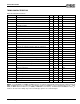
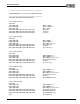
Specifications

ESS Technology, Inc. SAM0023-122898 85
ES1869 DATA SHEET
TIMING CHARACTERISTICS
TIMING CHARACTERISTICS
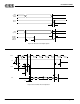
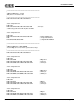
NOTE: * In Compatibility mode DMA, the DMA request is reset by the acknowledge signal going low. In Extended mode
DMA, the DMA request is reset when the acknowledge signal is low AND the correct command signal is low – either
IORB (for DMA read from I/O device) or IOWB (for DMA write to I/O device). For Extended mode DMA, the time t
10
is
relative to the later of the falling edge of the acknowledge signal or the command signal.
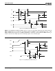
Table 29 Timing Characteristics
Symbol Parameter Min Typ Max Units
t
1
Reset pulse width 300 ns
t
2
IORB, IOWB pulse width 100 ns
t
3
Address setup time 10 ns
t
4
Read data access time 70 ns
t
5
Read data hold time 10 ns
t
6
Write data setup time 5 ns
t
7
Write data hold time 10 ns
t
8
DMA request to AEN high 0 ns
t
9
DMA request to DMA ACK 10 ns
t
10
DMA ACK to request release * 30 ns
t
11
DMA ACK high to AEN low 0 ns
t
12
DMA ACK to IOWB, IORB low 0 ns
t
13
IOWB, IORB to DMA ACK release 20 ns
t
14
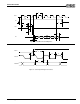
Crystal frequency, XI/XO 14.318 MHz
t
17
AEN, A[11:0], CDCSB0, CDCSB1, MMCSB, CDENB low 20 ns
t
18
AEN, A[11:0], CDCSB0, CDCSB1, MMCSB, CDENB high 20 ns
t
19
AEN, A[11:0], IOWB, IORB to GPO0, GPO1 delays 20 ns
t
20
SE high to valid FSR, FSX edge 2 DCLK
t
21
SE release time to Last DX, DR data bit 1 DCLK
t
22
SE, FSX, FSR setup time to DCLK edge 15 ns
t
23
SE, FSX, FSR, DR hold time to DCLK edge 10 ns
t
24
DX delay time from DCLK edge 20 ns
t
25
DX hold time from DCLK edge 10 ns
t
26
FSR, FSX pulse width 60 500 ns
t
27
DCLK clock frequency 2.04 MHz
t
28
IISCLK delay 2 ns
t
29
IISCLK setup 32 ns
t
30
Bit clock low 22 ns
t
31
Bit clock high 22 ns
t
32
Data setup time 32 ns
t
33
Data hold time 2 ns