
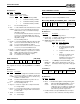
Specifications

70 SAM0023-122898 ESS Technology, Inc.
ES1869 DATA SHEET
REGISTERS
Audio 1 Control 2 (B8h, R/W)
Bit Definitions:
Audio 1 Transfer Type (B9h, R/W)
Bit Definitions:
Left Channel ADC Offset Adjust (BAh, R/W)
This register is reset to zero by hardware reset and is
unaffected by software reset.
Bit Definitions:
Right Channel ADC Offset Adjust (BBh, R/W)
This register is reset to zero by hardware reset and is
unaffected by software reset.
Bit Definitions:
Bits 4 (sign) and 3:0 (adjust magnitude) of the ADC Offset
Adjust registers cause a constant value to be added to the
ADC converter output, as shown in the following:
6 Set opposite
bit 3
Reserved function. This bit must be set to
the opposite polarity of bit 3: high for mono
and low for stereo.
5 FIFO signed
mode
1 = First DMA FIFO two’s complement mode
(signed data).
0 = First DMA FIFO unsigned (offset 8000).
4 1 Reserved. Always write 1.
3 FIFO stereo
mode
1 = First DMA FIFO stereo mode.
0 = First DMA FIFO mono mode.
Bit 6 must be set at the opposite polarity of
this bit: high for mono, low for stereo.
2 FIFO 16-bit
mode
1 = First DMA FIFO 16-bit mode.
0 = First DMA FIFO 8-bit mode.
1 0 Reserved. Always write 0.
0 Generate
load signal
Write 1. Generates a load signal that copies
DAC Direct Access Holding register to DAC
on the next sample rate clock edge (sample
rate is determined by Extended mode regis-
ter A1h). This bit is cleared after the holding
register is copied to the DAC.
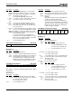
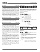
0 0 0 0
CODEC
mode
DMA
mode
DMA read
enable
DMA transfer
enable
7 6 5 4 3 2 1 0
Bits Name Description
7:4 0 Reserved. Always write 0.
3 CODEC
mode
1 = first DMA converter in ADC mode.
0 = first DMA converter in DAC mode.
2 DMA mode 1 = auto-initialize mode.
0 = normal DMA mode.
1 DMA read
enable
1 = first DMA is read (e.g. for ADC operation).
0 = first DMA is write (e.g. for DAC operation).
0 DMA
transfer
enable
First DMA active-low reset. When high, first
DMA is allowed to proceed.
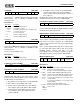
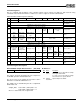
0 0 0 0 0 0 DMA transfer type select
7 6 5 4 3 2 1 0
Bits Name Description
7:2 0 Reserved. Always write 0.
Bits Name Description
1:0 DMA
transfer
type
select
Selects the DMA transfer type for the first DMA.
0 0
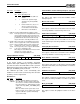
Disable time delay on
analog wake-up
Sign Adjust magnitude
7 6 5 4 3 2 1 0
Bits Name Description
7:6 0 Reserved. Always write 0.
5 Disable time
delay on
analog
wake-up
Normally, the AOUT_L and AOUT_R pins
are muted for 100 msec ± 20 msecs after
hardware reset or after the analog sub-
systems wake from power-down. Set high to
disable delay.
This bit is cleared by hardware reset.
4:0 Sign/Adjust
magnitude
See the explanation for bits 4:0 following
register BBh.
0 0 0 Sign Adjust magnitude
7 6 5 4 3 2 1 0
Bits Name Description
7:5 0 Reserved. Always write 0.
4:0 Sign/Adjust
magnitude
See the following explanation for bits 4:0.
Bits Name Description
Bit 1 Bit 0 Transfer Type
Bytes/DMA
Request
0 1 Single –
1 0 Demand 2
1 1 Demand 4
0 0 Reserved –