
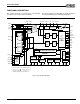
Specifications

ESS Technology, Inc. SAM0023-122898 7
ES1869 DATA SHEET
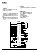
PIN DESCRIPTION
FOUT_L 45 O Filter output left. FOUT_L is AC-coupled externally to CIN_L to remove DC offsets. This out-
put has an internal series resistor of about 5k ohms. A capacitor to analog ground on this pin
can be used to create a low-pass filter pole that removes the switching noise introduced by
the switched-capacitor filter.
CIN_L 46 I Capacitive coupled input left. CIN_L has an internal pull-up resistor to CMR of approxi-
mately 50k ohms.
CIN_R 47 I Capacitive coupled input right. CIN_R has an internal pull-up resistor to CMR of approxi-
mately 50k ohms.
LINE_L 48 I Line input left. LINE_L has an internal pull-up resistor to CMR.
LINE_R 49 I Line input right. LINE_R has an internal pull-up resistor to CMR.
AOUT_L 50 O Line-level stereo output left. AOUT_L can drive a 10k ohm load.
AOUT_R 51 O Line-level stereo output right. AOUT_R can drive a 10k ohm load.
MMIEB
0
53
I Modem interrupt enable active-low input. Generated from the modem UART.
PCSPKO
1
O PC speaker analog output.
MMIRQ
0
54
I Modem interrupt request active-high input. IRQ input from the modem device gets mapped
to an IRQ output on the ES1869 based on the PnP configuration.
PCSPKI
1
I Normally low digital PC speaker input. This signal is converted to an analog signal with vol-
ume control and appears on analog output PCSPKO.
IISLR
1
55
I Left/right strobe for I
2
S interface. This pin has a pull-down.
MMCSB
0
O Output from ES1869 for the modem CSB. The address space is determined by the PnP
configuration.
GPCS
56
O If selected by the PnP logic, GPCS is an active-high user-defined chip select for an external
general-purpose device.
GPO0
O Output that is set low by external reset and is thereafter controlled by bit 0 of port
Audio_Base+7h. Available to system software for power management or other applications.
MSO 58 O MIDI serial data output.
MSI 59 I MIDI serial data input. Schmitt trigger input with internal pull-up resistor. Either MPU-401 or
Sound Blaster formats.
MODE 60 I Mode function pin. Connect to either GNDD or VDDD to select the function of the groups of
multiple function pins (indicated by a superscript 0 or 1).
DRQD
0
61
O Tri-state output. Optional 16-bit DMA request for IDE interface.
IISDATA
1
I Serial data for I
2
S interface. This pin has a pull-down.
DACKBD
0
62
I Optional 16-bit DMA acknowledge for IDE interface.
IISCLK
1
I Serial shift clock for I
2
S interface. This pin has a pull-down.
DRQ(A-C) 67,65,63 O Three (A,B,C) active-high DMA requests to the ISA bus. Unselected DRQ outputs are high
impedance. When DMA is not active, the selected DRQ output has a pull-down device that
holds the DRQ line inactive unless another device that shares the same DRQ line can
source enough current to make the DRQ line active. DRQs are software configurable.
DACKB(A-C) 68,66,64 I Three (A,B,C) active-low DMA acknowledge inputs.
IRQ(A-F) 69:74 O Six (A,B,C,D,E,F) active-high interrupt requests to the ISA bus. Unselected IRQ outputs are
high impedance. IRQs are software configurable.
IORB 75 I Active-low read strobe from the ISA bus.
IOWB 76 I Active-low write strobe from the ISA bus.
XI 78 I Crystal oscillator/external clock input. Connect to external 14.318 MHz crystal or clock
source with CMOS levels.
Name Number I/O Description