
Specifications

ESS Technology, Inc. SAM0023-122898 61
ES1869 DATA SHEET
REGISTERS
FSX/FSR Rate Control (Test) (4Ah, R/W)
Bit Definitions:
Serial Mode Filter Divider (4Ch, R/W)
This register controls the switched-capacitor filter during
Serial mode.
Bit Definitions:
Serial Mode Format/Source/Target (4Eh, R/W)
Bit Definitions:
4 Enable
ES689/
ES69x
intfc
1 = Enable ES689/ES69x to use music DAC if
MCLK is detected high at least once every 20
µsec. Mixer volume for this DAC is controlled by
the FM mixer volume register.
0 = Disable ES689/ES69x serial interface.
3 Active-
low
sync
1 = Frame sync pulses (FSR,FSX) are active-low.
0 = Frame sync pulses are active-high.
2 DSP
test
mode
Test mode. DCLK, FSX, and FSR become out-
puts. DCLK is 1.5876 MHz. FSX and FSR are
active-high frame syncs at a rate determined by
mixer register 4Ah.
1 Enable
1st
DMA in
SMODE
1 = Game and Telephony mode enabled. In Serial
mode, connect first channel DMA (game compati-
ble DMA) to second channel DAC. The second
channel DAC gets its filter clock and volume con-
trol from the first channel.
0 = Game and Telephony mode disabled. In
Serial mode, the first channel DMA does not get
played. The second channel DMA is connected to
the second channel DAC as usual.
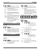
0 0 Reserved. Always write 0.
0 Two’s complement divisor
7 6 5 4 3 2 1 0
Bits Name Description
7 0 Reserved. Always write 0.
6:0 Two’s
comp
divisor
Used in a test mode enabled by bit 2 of mixer reg-
ister 48h. In this mode DCLK is a clock output of
1.5876 MHz. Bits 6:0 determine the rate of the
active-high frame sync outputs FSX and FSR.
Example: if bits 6:0 were programmed to be 5Ch
(-36 decimal), then the frame rate is 44.1 kHz.
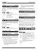
Filter override 0 0 0 Two’s complement filter divider
7 6 5 4 3 2 1 0
Bits Name Description
7 Filter
override
1 = During Serial mode, the first channel DAC
and ADC switched-capacitor filters are controlled
by a clock derived from DCLK.
0 = This register has no effect.
6:4 0 Reserved. Always write 0.
Bits Name Description
3:0 Two’s
comp
filter
divider
Bits 3:0 are a two's complement value that
divides down the DCLK input. The ratio of the fil-
ter -3 dB frequency to the filter clock is approxi-
mately 1:41.
Examples:
02h (-14) External Serial Clock 2.048 MHz/14/41
= 3568 Hz for 8000 Hz Sample Rate.
0Eh (-2) Internal Serial Clock 1.591 MHz/2/41
= 19.4 kHz for 44,100 Sample Rate. Note that the
sample rate divider is an integer multiple of the fil-
ter divide for 44,100, which gives maximum per-
formance of DACs and ADCs.
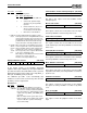
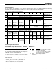
TX
SRC1
TX
SRC0
TX
16/8
TX
stereo/
mono
RX
SRC1
RX
SRC0
RX
16/8
RX
stereo/
mono
7 6 5 4 3 2 1 0
Bits Name Description
7:6 TX
SRC1/
SRC0
Transmit Register Source.
5 TX 16/8 1 = Transmit length is 16 bits.
0 = Transmit length is 8 bits.
4 TX
stereo/
mono
1 = Transmit mode is stereo. Left and right chan-
nels alternate, with left channel data preceding
right channel data.
0 = Transmit mode is mono.
3:2 RX
SRC1/
SRC0
Receive Register Target.
1 RX 16/8 1 = Receive length is 16 bits.
0 = Receive length is 8 bits.
0 RX
stereo/
mono
1 = Receive mode is stereo. Left and right chan-
nels alternate, with left channel data preceding
right channel data.
0 = Receive mode is mono.
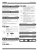
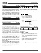
Bits Name Description
Bit 7 Bit 6 Source
0 0 None: tx register held at zero
0 1 1st channel DMA FIFO (1st chan-
nel in mono/stereo playback dir).
1 0 1st channel ADC (mono: L ch).
1 1 ----
Bit 3 Bit 2 Target
0 0 None: rx register held at zero
0 1 1st channel DMA FIFO (1st chan-
nel in mono/stereo record dir).
1 0 1st channel DAC (mono: R ch).
1 1 ----