
Specifications

42 SAM0023-122898 ESS Technology, Inc.
ES1869 DATA SHEET
I/O PORTS
FM Data Write (FM_Base+1h, W)
FM register write. The data written to FM_Base+1h is
written to the current address FM register. Note that
register writes must follow the timing requirements of the
OPL3 FM synthesizer.
FM High Bank Address (FM_Base+2h, W)
High bank register address.
FM Data Write (FM_Base+3h, W)
FM register write. Writing to this register in Emulation
mode is the same as writing to register FM_Base+1h.
MPU-401 Device
MPU-401 Data (MPU_Base+0h, R/W)
This register is used to read data from the MPU-401
receive FIFO or a command acknowledge byte (0FEh).
This register is also used to write data to the MPU-401
transmit FIFO.
MPU-401 Command (MPU_Base+1h, W)
The MPU-401 device accepts only two commands:
FFh Reset/return to Smart mode. This command
generates an acknowledge byte if received
when already in Smart mode.
3Fh Go to UART mode. This command generates
an acknowledge byte if received while in
Smart mode. It is ignored if the device is
already in UART mode.
MPU-401 Status (MPU_Base+1h, R)
Bit Definitions:
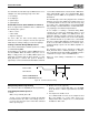
Joystick Device
The joystick device uses only a single I/O port. The device
can function in one of two modes: Analog mode or Digital
mode. The use of this I/O port is different depending on the
mode. This section describes Analog mode. Digital mode
is described in “Joystick / MIDI External Interface” on
page23.
Joystick_Base+0h (W)
Any value written to the Joystick_Base+0h port will restart
the timing sequence. This should be done before reading
the timer status flags.
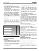
Joystick_Base+0h (R)
SW(A-D) return the current state of the joystick switch
inputs. T(A-D) return the current state of the four one-shot
timers connected to the X and Y resistors of the dual
joysticks.
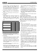
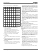
D7 D6 D5 D4 D3 D2 D1 D0
7 6 5 4 3 2 1 0
A7 A6 A5 A4 A3 A2 A1 A0
7 6 5 4 3 2 1 0
D7 D6 D5 D4 D3 D2 D1 D0
7 6 5 4 3 2 1 0
D7 D6 D5 D4 D3 D2 D1 D0
7 6 5 4 3 2 1 0
D7 D6 D5 D4 D3 D2 D1 D0
7 6 5 4 3 2 1 0
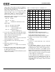
-RR -TR X X X X X X
7 6 5 4 3 2 1 0
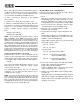
Bits Name Description
7 0 = read data available in the receive FIFO, or
pending acknowledge byte to be read (0FEh).
6 0 = there is room in the transmit FIFO to accept
another byte.
X X X X X X X X
7 6 5 4 3 2 1 0
SWD SWC SWB SWA TD TC TB TA
7 6 5 4 3 2 1 0