
Specifications

4 SAM0023-122898 ESS Technology, Inc.
ES1869 DATA SHEET
TABLES
Pop Prevention in the External Amplifier . . . . . . . . .77
Power Management and the FM Synthesizer . . . . .78
Self-Timed Power-Down . . . . . . . . . . . . . . . . . . . . . . . . .78
Enabling Self-Timed Power-Down . . . . . . . . . . . . . .78
General-Purpose Outputs and Power-Down . . . . . . . . .78
ELECTRICAL CHARACTERISTICS . . . . . . . . . . . . . . . . . . .79
Absolute Maximum Ratings . . . . . . . . . . . . . . . . . . . . . .79
Thermal Characteristics . . . . . . . . . . . . . . . . . . . . . . . . .79
Operating Conditions . . . . . . . . . . . . . . . . . . . . . . . . . . .79
Operating Current . . . . . . . . . . . . . . . . . . . . . . . . . . . . . .79
TIMING DIAGRAMS . . . . . . . . . . . . . . . . . . . . . . . . . . . . . . .80
TIMING CHARACTERISTICS . . . . . . . . . . . . . . . . . . . . . . . .85
MECHANICAL DIMENSIONS . . . . . . . . . . . . . . . . . . . . . . . .86
ES1869F PQFP Package . . . . . . . . . . . . . . . . . . . . . . . 86
ES1869S TQFP Package . . . . . . . . . . . . . . . . . . . . . . . 87
APPENDIX A: ES1869 PNP ROM DATA EXAMPLE . . . . . . 88
APPENDIX B: ES689/ES69X DIGITAL SERIAL INTERFACE .
92
APPENDIX C: I
2
S ZV INTERFACE REFERENCE . . . . . . . . 93
APPENDIX D: MOTHERBOARD SCHEMATICS . . . . . . . . . 98
APPENDIX E: MOTHERBOARD BILL OF MATERIALS . . 102
APPENDIX F: SOUND CARD SCHEMATICS . . . . . . . . . . 104
APPENDIX G: SOUND CARD BILL OF MATERIALS . . . . 108
APPENDIX H: LAYOUT GUIDELINES . . . . . . . . . . . . . . . . 110
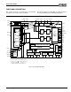
FIGURESFigure 1 Typical Application . . . . . . . . . . . . . . . . . .2
Figure 2 ES1869F Pinout (PQFP Package) . . . . . . . . . . . . . .5
Figure 3 ES1869S Pinout (TQFP Package) . . . . . . . . . . . . . .5
Figure 4 ES1869 Block Diagram . . . . . . . . . . . . . . . . . . . . . . .9
Figure 5 ES1869 Mixer Schematic Block Diagram . . . . . . . . 11
Figure 6 Data Transfer Modes . . . . . . . . . . . . . . . . . . . . . . .13
Figure 7 DRQ Latch . . . . . . . . . . . . . . . . . . . . . . . . . . . . . . .15
Figure 8 I
2
S Implementation in ES1869 . . . . . . . . . . . . . . . .19
Figure 9 Telegaming Mode . . . . . . . . . . . . . . . . . . . . . . . . . .20
Figure 10 Default Mode . . . . . . . . . . . . . . . . . . . . . . . . . . . . .20
Figure 11 16-Bit Data, Positive Sync Pulse . . . . . . . . . . . . . .21
Figure 12 Speakerphone or Modem w/ Voice-Over-Data . . .22
Figure 13 IDE Interface – Typical Application . . . . . . . . . . . .22
Figure 14 Dual Joystick/MIDI Connector . . . . . . . . . . . . . . . .23
Figure 15 MIDI Serial Interface . . . . . . . . . . . . . . . . . . . . . . .24
Figure 16 Serial EEPROM – Typical Application . . . . . . . . .24
Figure 17 PC Speaker Volume Circuitry . . . . . . . . . . . . . . . .26
Figure 18 Reference Generator Pin Diagram . . . . . . . . . . . .27
Figure 19 Switch-Capacitor Filter Pin Diagram . . . . . . . . . . .27
Figure 20 Configuration Register Set . . . . . . . . . . . . . . . . . .28
Figure 21 Command Transfer Timing . . . . . . . . . . . . . . . . . .45
Figure 22 Summary of Power States in the ES1869 . . . . . . .75
Figure 23 Reset Timing . . . . . . . . . . . . . . . . . . . . . . . . . . . . .80
Figure 24 I/O Read Cycle . . . . . . . . . . . . . . . . . . . . . . . . . . .80
Figure 25 I/O Write Cycle . . . . . . . . . . . . . . . . . . . . . . . . . . .80
Figure 26 Compatibility Mode DMA Write Cycle . . . . . . . . . 81
Figure 27 Compatibility Mode DMA Read Cycle . . . . . . . . . 81
Figure 28 Miscellaneous Output Signals . . . . . . . . . . . . . . . 82
Figure 29 Serial Mode Receive Operation . . . . . . . . . . . . . . 82
Figure 30 Serial Mode Transmit Operation . . . . . . . . . . . . . 83
Figure 31 Serial Input Timing for I
2
S Interface . . . . . . . . . . . 83
Figure 32 I
2
S Digital Input Format with 16 SCLK Periods . . 84
Figure 33 ES1869F PQFP Mechanical Dimensions . . . . . . 86
Figure 34 ES1869S TQFP Mechanical Dimensions . . . . . . 87
Figure 35 Example ZV Port Implementation . . . . . . . . . . . . 93
Figure 36 Typical ZV Port Audio Implementation . . . . . . . . 94
Figure 37 Audio Interface Timing . . . . . . . . . . . . . . . . . . . . . 95
Figure 38 I
2
S Digital Input Format with 16 SCLK periods . . 96
Figure 39 ES1869 – Motherboard Configuration . . . . . . . . . 98
Figure 40 ES1869 and ES692 – Motherboard Configuration 99
Figure 41 Amplifier – Motherboard Configuration . . . . . . . 100
Figure 42 PC Interface – Motherboard Configuration . . . . 101
Figure 43 ES1869 – Sound Card Configuration . . . . . . . . 104
Figure 44 ES1869 and ES692 – Sound Card Configuration 105
Figure 45 Amplifier – Sound Card Configuration . . . . . . . . 106
Figure 46 PC Interface – Sound Card Configuration . . . . . 107
Figure 47 Analog Components on One Side of the PCB . . 110
Figure 48 Analog Components on Both Sides of the PCB 110
TABLES
Table 1 ISA Bus Interface Pins . . . . . . . . . . . . . . . . . . . . . . .12
Table 2 Extended Mode Audio 1 Controller Registers . . . . .14
Table 3 Audio 2 Related Mixer Registers . . . . . . . . . . . . . . .15
Table 4 ES1869 Interrupt Sources . . . . . . . . . . . . . . . . . . . .17
Table 5 Interrupt Status Bits in Config_Base+6h . . . . . . . . .17
Table 6 I
2
S Interface Pins . . . . . . . . . . . . . . . . . . . . . . . . . . .19
Table 7 Wavetable Interface Pins . . . . . . . . . . . . . . . . . . . . .19
Table 8 DSP Interface Pins . . . . . . . . . . . . . . . . . . . . . . . . . .19
Table 9 External Modem Interface Pins . . . . . . . . . . . . . . . .22
Table 10 IDE CD-ROM Interface Pins . . . . . . . . . . . . . . . . . .22
Table 11 Logical Device Summary . . . . . . . . . . . . . . . . . . . .31
Table 12 I/O Ports for Configuration, Audio, FM, MPU-401,
and Joystick Devices . . . . . . . . . . . . . . . . . . . . . . . . . . . . .38
Table 13 Comparison of Operation Modes . . . . . . . . . . . . . .44
Table 14 Uncompressed DAC Transfer Modes . . . . . . . . . . .46
Table 15 Uncompressed ADC Transfer Modes . . . . . . . . . . .47
Table 16 Command Sequences for DMA Playback . . . . . . .49
Table 17 Command Sequence for DMA Record . . . . . . . . . .50
Table 18 Sound Blaster Pro/Extended Access Registers . . .53
Table 19 SB Pro Read Volume Emulation . . . . . . . . . . . . . . 54
Table 20 SB Pro Write Volume Emulation . . . . . . . . . . . . . . 54
Table 21 Extended Access Mixer Volume Values . . . . . . . . 55
Table 22 Mixer Input Volume Registers . . . . . . . . . . . . . . . . 55
Table 23 Sound Blaster Compatibility Register Summary . . 56
Table 24 ESS Mixer Registers Summary . . . . . . . . . . . . . . . 57
Table 25 ESS Controller Registers Summary . . . . . . . . . . . 67
Table 26 Command Summary . . . . . . . . . . . . . . . . . . . . . . . 72
Table 27 Digital Characteristics . . . . . . . . . . . . . . . . . . . . . . 79
Table 28 Analog Characteristics . . . . . . . . . . . . . . . . . . . . . 79
Table 29 Timing Characteristics . . . . . . . . . . . . . . . . . . . . . . 85
Table 30 Common Clock Frequencies . . . . . . . . . . . . . . . . . 94
Table 31 AC Parameters for Audio Signals . . . . . . . . . . . . . 95
Table 32 ZV Port Interface Pin Assignments . . . . . . . . . . . . 97
Table 33 ES1869 Motherboard Bill of Materials (BOM) . . . 102
Table 34 ES1869 Sound Card Bill of Materials (BOM) . . . 108