
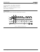
Specifications

ESS Technology, Inc. SAM0023-122898 27
ES1869 DATA SHEET
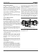
ANALOG DESIGN CONSIDERATIONS
ANALOG DESIGN CONSIDERATIONS
This section describes design considerations related to
inputs and outputs of analog signals and related pins on
the chip.
Game Port
The game port address 201h is decoded for timer pins TA,
TB, TC, and TD, and switch pins SWA, SWB, SWC, and
SWD. The MIDI serial input and output also come from the
game port connector in most applications.
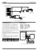
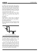
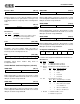
Reference Generator
Reference generator pin CMR is shown bypassed to
analog ground.
Figure 18 Reference Generator Pin Diagram
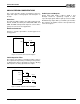
Switch-Capacitor Filter
The outputs of the FOUT_L and FOUT_R filters must be
AC-coupled to the inputs CIN_L and CIN_R. This provides
for DC blocking and an opportunity for low-pass filtering
with capacitors to analog ground at these inputs.
Figure 19 Switch-Capacitor Filter Pin Diagram
Audio Inputs and Outputs
Analog inputs MIC, LINE_L, LINE_R, AUXA_L, and
AUXA_R should be capacitively coupled to their
respective input signals. All have pull-up resistors to CMR.
ES1869 analog outputs AOUT_L and AOUT_R should be
AC-coupled to an amplifier, volume control potentiometer,
or line-level outputs.
ES1869
CMR
47 µF
.1 µF
+
ES1869
FOUT_L
CIN_L
.22 µF
.22 µF
FOUT_R
CIN_R
680 pF
680 pF